Magnetic domains walls are known to be a source of electrical resistance due to the difficulty for transport electron spins to follow their magnetic texture. This phenomenon holds potential for utilization in spintronic devices, where the electrical resistance can vary based on the presence or absence of a domain wall. A particularly intriguing class of materials are half metals such as La2/3Sr1/3MnO3 (LSMO) which present full spin polarization, allowing their exploitation in spintronic devices. Still the resistance of a single domain wall in half metals remained unknown. Now a team from Spain, France and Germany has generated a single domain wall on a LSMO nanowire and measured resistance changes 20 times larger than for a normal ferromagnet such as Cobalt.
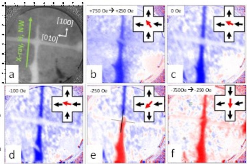
 Magnetic sensitive PEEM images obtained at HZB: a) XAS image of the crossed nanowires. X-ray beam and magnetic field are aligned along the nanowire(vertical) direction (green arrow). b-f) XMCD images of the cross for different applied fields. Image Credit: © HZB
The magnetic domain texture inherent to magnetic domain walls holds potential for spintronic applications. The electrical resistance in ferromagnets depends on whether domain walls are or not present. This binary effect (known as domain wall magnetoresistance) could be used to encode information in spintronic memory devices. Yet, their exploitation is hindered due to the small changes in resistance observed for normal ferromagnets. A particularly interesting class of materials are manganite perovskites such as La2/3Sr1/3MnO3 (LSMO). These compounds present only one type of spin (full spin polarization) which could potentially lead to domain wall magnetoresistance effects large enough to be exploited in a new generation of spintronic sensors and injectors.
Despite this promising perspective, there exist large discrepancies in the reported values of the domain wall magnetoresistance for this system. The scientists from Spain, France and Germany have fabricated nanowire-based devices enabling the nucleation of individual magnetic domain walls. Magneto transport measurements in these devices show that the presence of a domain wall leads to an increase of the electrical resistance of up to 12%. In absolute terms, the observed resistance change is 20 times larger than that reported for Cobalt.
This work is the result of a longstanding collaboration which involves film growth and nanofabrication, transport measurements, contact microscopy (MFM) imaging, theoretical simulations and the use of advanced characterization techniques such as X-ray photoemission electron microscopy. The combination of a wide variety of different techniques provides a comprehensive multi-facet view of a complex problem which has allowed to reach new insights into a highly debated open question.