Oct 16 2007
IBM scientists have announced that they have measured the distribution of electrical charges in tubes of carbon that measure less than 2 nanometers in diameter, 50,000 times thinner than a strand of human hair.
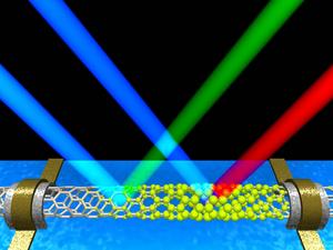
 Vibrations give color to light allowing us to locally measure charges in a nanoscale electronic device.
This novel technique, which relies on the interactions between electrons and phonons, provides a detailed understanding of the electrical behavior of carbon nanotubes, a material that shows promise as a building block for much smaller, faster and lower power computer chips compared to today's conventional silicon transistors.
Phonons are the atomic vibrations that occur inside material, and can determine the material's thermal and electrical conductivity. Electrons carry and produce the current. Both are important features of materials that can be used to carry electrical signals and perform computations.
The interaction between electrons and phonons can release heat and impede electrical flow inside computer chips. By understanding the interaction of electrons and phonons in carbon nanotubes, the researchers have developed a better way to measure their suitability as wires and semiconductors inside of future computer chips.
In order to make carbon nanotubes useful in building logic circuitry, scientists are pushing to demonstrate their high speed, high packing density and low power consumption capabilities as well as the ability to make them viable for potential mass production.
"The success of nanoelectronics will largely depend on the ability to prepare well characterized and reproducible nano-structures, such as carbon nanotubes," said Dr. Phaedon Avouris, IBM Fellow and lead researcher for IBM's carbon nanotube efforts. "Using this technique, we are now able to see and understand the local electronic behavior of individual carbon nanotubes."
To date, researchers have been able to build carbon nanotube transistors with superior performance, but have been challenged with reproducibility issues. Carbon nanotubes are sensitive to environmental influences. For example, their properties can be altered by foreign substances, affecting the flow of electrical current and changing device performance. These interactions are typically local and change the density of electrons in the various devices of an integrated circuit, and even along a single nanotube.
A better understanding of how the local environment affects the electrical charge of a carbon nanotube is needed to allow the fabrication of more reliable transistors. Therefore, the ability to measure local electron density changes in a nanotube is essential. A team of researchers from the IBM's T.J. Watson Research Center in Yorktown Heights have just solved this problem.
This achievement was published online October 14, 2007 in the journal Nature Nanotechnology. The team monitored the color of the light scattered from the nanotube (Raman Effect), and measured small changes in the color of the light corresponding to changes in the electron density in the nanotube. The technique takes advantage of the interaction between the motion of the atoms and the motion of the electrons, so that electron density changes can be reflected in changes of the frequency of the vibrational motion of the nanotube atoms.
In March 2006, IBM announced that its researchers built the first complete electronic integrated circuit around a single carbon nanotube molecule.
For more information about IBM Research, visit http://www.research.ibm.com/.