Oct 23 2008
Leaders of the chip making industry have assembled in Austin, Texas this week to examine, in part, equipment productivity at the ISMI Symposium On Manufacturing Effectiveness, including details presented by Dennis J. Bonciolini -- the CTO of CyberOptics Semiconductor -- of a 300mm fab's implementation of wireless machine-vision devices to teach robot wafer-transfer coordinates and improve tool production time 600 percent.
 Leaders of the chip making industry have assembled in Austin, Texas this week, in part, to examine equipment productivity at the ISMI Symposium On Manufacturing Effectiveness, including details presented by the CTO of CyberOptics Semiconductor of a 300mm fab's implementation of wireless machine-vision devices to teach robot wafer-transfer coordinates and improve tool production time 600 percent.
At the 5th annual symposium, which offers attendees information to reduce manufacturing expenses and increase productivity, Bonciolini will discuss how process engineers working with an Endura platform vented or cooled process chambers during attempts to establish wafer-transfer coordinates for teaching robots. The engineers essentially operated without the proper tools to identify targets inside equipment.
The process engineers' manual teaching methods led to extended equipment setup and maintenance time, human interference and avenues for wafer particulate contamination, according to the company, a subsidiary of CyberOptics Corp. (NASDAQ: CYBE).
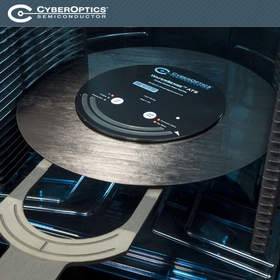
Bonciolini's presentation will address how the fab implemented a wafer-like device that uses machine-vision technology to capture real-time shots of critical targets with the Endura. The device's on-board camera obtained live video and reported in real-time the device's coordinates in relation to a target via companion software.
The device allowed the chip maker to save 20 hours of equipment time, according to Bonciolini. He added that the chip maker implemented the device at tools fab-wide after obtaining data from the implementation.
Bonciolini will deliver his presentation titled "A Case Study for Improved Robot Teaching Methodology On 300mm Endura" on Wednesday, Oct. 22 at 2:25 p.m. at the Bergstrom Ballroom BC in the Hilton Austin Airport. The abstract can be viewed here: http://ismi.sematech.org/ismisymposium/abstracts/06041613039.pdf. Bonciolini was also a guest speaker this week at two ISMI workshops on predictive maintenance and second source parts.
"This is really a great event for suppliers and manufacturers to get together and address industry challenges, and I'm certainly glad we'll be able to contribute and talk about our experience teaching robots in the Endura cluster tool," Bonciolini said.
The device featured in the presentation, the WaferSense Auto Teaching System (ATS), obtains the three-axis (x, y, z) coordinates needed to establish optimal transfers and uniform process results.
CyberOptics Semiconductor, a maker of wireless metrology devices for wafer processing equipment, will demonstrate the ATS and its entire line of WaferSense products at the symposium, including its Auto Vibration System (AVS), Auto Leveling System (ALS2 Vertical) and Auto Gapping System (AGS). Each device follows the processing life of a wafer and reports real-time metrology data.
The ATS is available in 200 and 300 mm form factors and has an accuracy of +/-0.1 mm (X and Y positions) and +/-0.5 mm (Z position).
The WaferSense ATS package includes the teaching wafer, USB-compatible link, TeachView™ and TeachTarget™ software CD, charging case and suitcase.