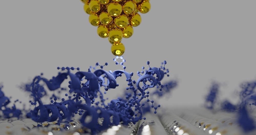
Atomic force microscopy (AFM) is a versatile microscopic technology used for analyzing various samples at the nanoscale dimension. This analytical tool not only offers a three-dimensional image of the sample’s surface but also assists in its manipulation at the nanoscale.

Image Credit: sanjaya viraj bandara/Shutterstock.com
The most important part of this instrument is its tip/ cantilever, also known as a probe. This tip interacts with the sample and generates useful data scientists require to analyze the sample.
AFM provides high-resolution three-dimensional imaging using the probe-sample interaction force as a feedback signal. This analytical tool is used to study glass, polymers, ceramics, composites, and biological samples. It is also used to determine different characteristics of a sample, such as its magnetic and mechanical properties.
Development of Nanotips used in Atomic Force Microscopy
Two of the most common materials used for developing AFM tips are silicon and silicon nitride. Most favorable tips possess ultra-high sharpness, great density, and a high aspect ratio. These characteristic features are associated with the production of high-resolution images.
Smaller nanotips permit rapid operational speed. AFM probes can be tuned using the micromachining technique, offering greater sensitivity, resonant frequency, and other important characteristic features to the nanotip. Two recently developed AFM probe fabrication techniques are top-down and bottom-up approaches.
Typically, a top-down approach is used for most AFM tip fabrication, e.g., silicon tip fabrication.
Silicon tips are fabricated using wet or dry etching from the top, promoting the production of small tip radius probes. One of the limitations of this technique is that it provides a low aspect ratio image.
Additionally, the tip sharpening method associated with the top-down approach is incompatible with other integration techniques as it requires high temperature.
On the other hand, carbon nanotube probes are created using a bottom-up fabrication technique, and this offers a high aspect ratio and a very sharp nanotip. This approach also includes some limitations, such as requiring a high-temperature environment for fabrication which is not compatible with different integration techniques.
Scientists have developed ultra-sharp sputtered Aluminum (Al) AFM tip fabrication techniques that can yield a high amount of AFM nanotips of radius ranging between 5nm and 100nm, by varying process parameters. This method produces smaller cantilevers for the AFM system, promoting a high-speed and high-density operation. Researchers indicated that this technique could be used to fabricate an array of AFM nanotips with an ultra-sharp high aspect ratio compatible with different integration processes.
Recently, scientists have developed MHz AFM nanoprobes with capacitive transducers vibrating in the in-plane elliptic mode. This type of nanotip consists of silicon ring resonators that generate high resonance frequency AFM images.
AFM nanotips are sometimes coated or functionalized with metals such as cobalt and platinum. Scientists coat AFM nanotips with metals when they require electrical or magnetic measurements. Probes are also sometimes functionalized with gold for biological applications.
Tungsten wire AFM nanoprobes are capable of high-resolution imaging of samples having very low ionic currents through pores. These AFM nanotips are coated with non-conducting materials on the probe tip. This enables the recording of small ionic currents flowing through the pores. This probe is used for imaging the nanostructure surface of biomolecules.
Different Shapes and Materials of AFM Nanotips
The material of the probe influences the function of AFM. For instance, a silicon probe can be made sharper but wears off faster than a probe made of silicon nitride. At present, researchers can obtain an AFM nanotip of their choice from a manufacturer or distributor. AFM nanotips are also made up of diamond, and the most important aspect of this type of probe is that it is wear-resistant. Additionally, these probes can hold their shape stably during imaging and provide improved and accurate electrical measurements.
Often researchers design probes of different shapes such as a cone, punch, sphere, plateau, rectangle, etc., to extract maximum material properties.
A tip shape is measured by blind reconstruction. However, the shape of the tip invariably changes during the course of an experiment. Expectantly, the shape of the tip wears off while imaging a hard sample or gets contaminated while analyzing a soft or sticky sample like a polymer. Scientists stated that shape of nanotip changes in real-time, and sometimes it might break while performing an experiment or may become sharper.
Researchers select suitable AFM nanotips in accordance with the experiment at hand. For instance, non-rotated types of polygon-based shaped AFM nanotips are located close to the free-end AFM cantilever. Typically, the height of the tip is 10-15 µm and the half cone angle is smaller than 10° at the apex. Sometimes similarly structured nanotips can rotate, known as rotated AFM tips.
Deep trenches of a nanostructure are measured using tilted focused ion beam AFM nanotips. The tilted high aspect ratio compensates for the mounting angle within the AFM head. Another type of AFM nanotip used to measure deep trenches is electron beam deposited extratips with varying geometry.
The gold-coated AFM nanotips are electrically conductive and are biocompatible.
Continue reading: Why AFM Is Critical To Graphene Research
References and Further Reading
Yadav, H and Sharma, M. (2020) Fabrication of Nano-Scale Ultra Sharp Atomic Force Microscopy (AFM) Tips. Journal of Critical Reviews. 7(3). Available at: https://www.bibliomed.org/fulltextpdf.php?mno=120354
Meckes, B., et al. (2014) Insulated Conducting Cantilevered Nanotips and Two-Chamber Recording System for High Resolution Ion Sensing AFM. Scientific Reports. 4, 4454. Available at: https://doi.org/10.1038/srep04454
Walter, B. et al. (2011) 4.8 MHz AFM nanoprobes with capacitive transducers and batch-fabricated nanotips. 2011 IEEE 24th International Conference on Micro Electro Mechanical Systems. pp. 517-520. Available at: https://ieeexplore.ieee.org/document/5734475
Disclaimer: The views expressed here are those of the author expressed in their private capacity and do not necessarily represent the views of AZoM.com Limited T/A AZoNetwork the owner and operator of this website. This disclaimer forms part of the Terms and conditions of use of this website.