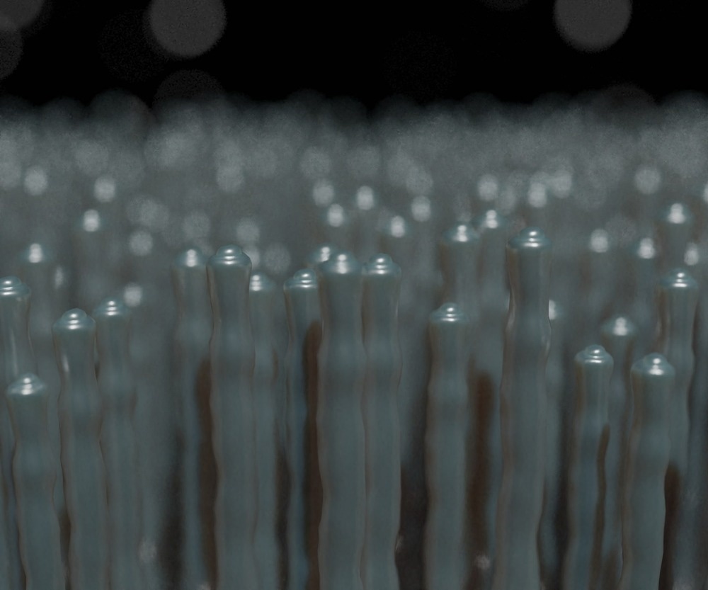
Raman spectroscopy is a non-invasive quantitative assessment method that offers extensive information on chemical composition, phases, crystalline structure, and molecular dynamics. Raman spectroscopy may determine the phases and phase changes of different nanomaterials, such as nanowires. This article outlines Raman spectroscopy's uses in the investigation of nanowires.

Image Credit: Love Employee/Shutterstock.com
Raman Spectroscopy and Nano Research: An Overview
Raman spectroscopy is a diagnostic method that uses scattered light to assess a sample's vibrational energy modes. It takes advantage of a concept called the Raman effect, which happens when a molecule's electric dipole is excited.
Raman spectroscopy may offer unique physical and chemical information, as well as identify compounds based on their Raman frequencies. These distinct dispersed frequencies may also be utilized to deduce the composition and attributes of the material under examination.
Raman spectroscopy has emerged as a popular tool of characterization in nanotechnology. The fundamental reason for this is because Raman spectroscopy can not only establish the composition of each nanomaterial, enabling it to be recognized, but it can also often discern the structural arrangement that differentiates two distinct forms of the same kind of nanomaterial.
Significance and Applications of Nanowires (NWs)
A nanowire is a nanoscale structure in the shape of a wire with a diameter of 10--9 meters or less. More broadly, nanowires are structures with a thickness or width limited to tens of nanometers and an unbound length.
Nanowires (NWs) may be produced from various materials, including silicon, germanium, carbon, and conducting metals like gold and copper. Because of their tiny size, they are strong conductors, allowing electrons to travel readily through them, leading to significant improvements in computer technology.
Compared to other nanomaterials, nanowires are of special importance owing to their asymmetric structure, which allows for controlling quantum effects in the short direction (diameter) while retaining bulk features, such as fast carrier transport, in the longer direction.
Raman Spectroscopy for Analysis of Nanowires
Semiconductor nanowires (NWs) have lately sparked considerable attention as building blocks for innovative nanoscale electronics. As physical qualities vary with size, NWs have numerous distinct features compared to their bulk counterparts.
Raman scattering is a non-destructive viscoelastic light scattering method that evaluates basic NW characteristics such as crystalline phases, electronic structures, structure, and strain field.
Carriers and phonon confinement are two of the most basic features seen in nanostructures such as nanowires. Confinement is often associated with designing different physical features, leading to innovative applications.
Raman spectroscopy is an excellent and very simple tool for testing this quantum confinement. This is because it can be realized under a wide range of severe and non-extreme circumstances, resulting in an excellent procedure for studying nanowires at both low and high temperatures and pressures.
Use of Raman Spectroscopy in Nanowire Research: Recent Advances
Raman spectroscopy has been extensively employed to analyze nanowires and quantum dots during the past decade, and various novel phenomena involving one-dimensional nanostructures have been documented to date.
Yakunin et al. used Raman spectroscopy to explore silicon nanowires formed by metal-assisted chemical treatment of crystalline silicon (Si) wafers to disclose the influence of nanowire production time and further doping with boron and phosphorus.
The observed alteration of the spectrum shape in boron-doped samples owing to the Fano effect allowed the density of free holes in Si nanowires to be estimated. The obtained findings show that Raman spectroscopy has the potential to be used for contactless monitoring of Si nanostructures.
In another study, Khanna et al. reported a new and simple approach for fabricating titanium dioxide (TiO2) nanowires as electrode material for supercapacitors. The creation of a rutile phase with a sufficient length and diameter was confirmed using Raman spectroscopy as the nanostructure grew at varying concentrations.
The TiO2 nanowire arrays produced on a Nitinol substrate demonstrated extremely strong specific capacitance and long-term durability, making it a possible contender for supercapacitor applications.
Benefits of Raman Spectroscopy for Nanowire Analysis
Raman spectroscopy is a flexible and widely used method for material characterization, providing extensive information on crystalline structure, phonon scattering, electronic properties, composition, and strain of nanowires.
As Raman spectroscopy may be carried out experimentally at the nanoscale using a fluorescent microscope or even a tip-enhanced scanning lens, submicron resolutions of the basic characteristics of nanoscale materials such as nanowires can be obtained using this method.
The use of Raman spectroscopy for nanowire investigation constitutes a very busy and fascinating topic for advancing science and technology at the nanoscale. This emerging new phenomenon has the potential to open new doors not just for the characterization of nanowires but also for the comprehension of basic processes connected to other nanoscale materials.
References and Further Reading
Chen, N. et al. (2020). Porous carbon nanowire array for surface-enhanced Raman spectroscopy. Nature Communications. Available at: https://doi.org/10.1038/s41467-020-18590-7
Khanna, S. et al. (2022). Fabrication of rutile – TiO2 nanowire on shape memory alloy: A potential material for energy storage application. Materials Today: Proceedings. Available at: https://doi.org/10.1016/j.matpr.2021.01.012
Matteis, D. et al. (2020). Probing Lattice Dynamics and Electronic Resonances in Hexagonal Ge and SixGe1–x Alloys in Nanowires by Raman Spectroscopy. ACS Nano. Available at: https://doi.org/10.1021/acsnano.0c00762
Yakunin, V. et al. (2019). Raman spectroscopy of silicon nanowires formed by metal-assisted chemical etching. Journal of Physics. Available at: https://iopscience.iop.org/article/10.1088/1742-6596/1348/1/012025
Disclaimer: The views expressed here are those of the author expressed in their private capacity and do not necessarily represent the views of AZoM.com Limited T/A AZoNetwork the owner and operator of this website. This disclaimer forms part of the Terms and conditions of use of this website.