The UK’s first dedicated electron diffraction center is due to open in the Summer of 2023. The new facility will help UK nanoscientists to characterize the "tiniest of crystals", according to Derek Wann, an electron diffraction expert at the University of York. The project team delivering the new center says that it will significantly impact the UK’s chemical industry, including its manufacturing, pharmaceuticals, and electronics sub-sectors.

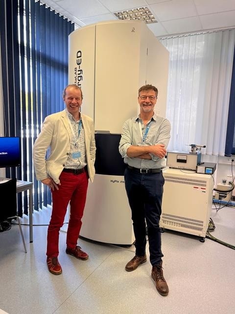
The University of Warwick’s Richard Beanland (right) with Simon Coles (left), who will head up the Southampton arm of the UK’s new electron diffraction centre. Image Credit: University of Southampton
With a government grant of £3.2 million from the Engineering and Physical Sciences Research Council (EPSRC), the National Electron Diffraction Facility will be established in 2023.
The facility is delivered by the National Crystallography Service (NCS), a joint effort between the UK’s University of Southampton and University of Warwick. As a vital component of the country’s research infrastructure, the NCS has facilitated numerous scientific discoveries and advancements, and this new center promises to enhance its capabilities further.
Featuring two of Rigaku's pioneering XtaLAB Synergy-ED diffractometers, the center will be housed in newly refurbished laboratories at Southampton and Warwick university campuses.
These cutting-edge instruments will be complemented by sample preparation facilities and ample space for visiting researchers to work and collaborate with the NCS team.
Thanks to the diffractometers’ user-friendly interface and software, which are identical to the x-ray diffraction systems currently in use at the NCS, transitioning to electron diffraction will be relatively straightforward in terms of skills development for researchers.
The center is due to open its doors to academic and commercial partners in July 2023.
What is Electron Diffraction?
Electron diffraction, akin to its standard gold counterpart, X-Ray diffraction, plays a crucial role in determining crystal structures. Unlike X-Rays, electron diffraction employs an electron beam to scatter off a sample's crystal lattice, generating a diffraction pattern that provides insight into the material's structural arrangement at the atomic level.
In electron diffraction, the incoming electrons interact with the electrostatic potential of the constituent atoms of the sample material, causing scattering that can then be used to identify the characteristics of the sample.
Electrons have a much shorter wavelength than X-rays, which means that the achievable resolution of electron imaging is significantly higher than that of X-ray techniques.
The Importance of Electron Diffraction to Nanoscience
Electron diffraction has become a powerful tool in nanoscience, often used in transmission electron microscopy (TEM) to study thin samples ranging from tens to, at most, a thousand atoms in thickness.
Electron diffraction is also utilized as electron backscatter diffraction in scanning electron microscopy (SEM) to determine crystal orientation and gas electron diffraction to characterize molecules in a gas.
In addition to TEM, electron diffraction can be used to characterize surfaces using lower energy electrons or by reflecting electrons off surfaces, a technique called RHEED.
The XtaLAB Synergy-ED is a new product for electron diffraction applications created by a collaboration between Rigaku Corporation and JEOL, two leading Japanese instrument manufacturers in X-Ray analysis and electron microscopy, respectively. This platform enables researchers to study crystalline materials that were previously difficult or impossible to measure by X-Ray diffraction techniques.
With this new instrument, UK nanoscientists can explore the structure of many economically important materials, including pharmaceuticals, catalysts, batteries, and energy storage materials.
The potential applications of electron diffraction are wide-ranging, particularly in the study of nanocrystals. In the National Electron Diffraction Facility, equipped with the XtaLAB Synergy-ED, UK researchers have a powerful new tool that can open up possibilities in the field of materials science.
Nanotechnology in the UK
The precise determination of 3D molecular structures at the atomic level is an important technique that drives innovation in various fields, such as drug discovery, synthetic chemistry, and material science.
The UK is already a well-established region for nanotechnology, being home to numerous world-renowned academic research institutions and market-leading nanotechnology companies.
Currently, the UK invests around 1.67% of its GDP in research and design into nanotechnology, and over 100 companies are operating in the UK nanotechnology market.
The UK holds a distinguished position in the research of graphene and carbon nanotechnology. The University of Manchester, in particular, has consistently maintained its prominence as a hub for global research on graphene since its own researchers initially characterized this two-dimensional material several decades ago. In 2022, UK government funding bodies invested £29 million in graphene and carbon nanotechnology research through university grants.
The new facility will enable more cutting-edge nanotechnology research to be completed in UK’s institutions, and could open up additional opportunities beyond advancing research in 3D molecular structures.
Electron beams are versatile phenomena, and the new center may enable more development and commercialization of novel electron sources.
The new facility is another jewel in the crown of UK nanotechnology and nanoscience research. The country’s strong advanced manufacturing, pharmaceuticals, and electronics sectors will expect it to deliver benefits soon.
References and Further Reading
Electron Diffraction. (2016) [Online] Encyclopedia Britannica. Available at: https://www.britannica.com/science/electron-diffraction.
Moore, S. (2019). Nanotechnology in the United Kingdom Market Report. [Online] AZO Nano. Available at: https://www.azonano.com/article.aspx?ArticleID=5385.
Pilkington, B. (2021). UK Government Bodies Behind Nanotechnology Research Funding. [Online] AZO Nano. Available at: https://www.azonano.com/article.aspx?ArticleID=6214.
Rigaku and JEOL Launch a Revolutionary Electron Diffraction Platform XtaLAB Synergy-ED. (2021) [Online] Rigaku. Available at: https://www.rigaku.com/press/tue-05252021-1200/192631151.
Urquhart, J. (2023). UK national facility poised to expand use of state-of-the-art electron diffraction. [Online] Chemistry World. Available at: https://www.chemistryworld.com/news/uk-national-facility-poised-to-expand-use-of-state-of-the-art-electron-diffraction/4017043.article
Simoncic, P. et al. (2023) ‘Electron crystallography and dedicated electron-diffraction instrumentation’, Acta Crystallographica Section E Crystallographic Communications, 79(5), pp. 410–422. doi:10.1107/s2056989023003109.
Disclaimer: The views expressed here are those of the author expressed in their private capacity and do not necessarily represent the views of AZoM.com Limited T/A AZoNetwork the owner and operator of this website. This disclaimer forms part of the Terms and conditions of use of this website.