Nov 27 2009
The EU's SMARTIEHS project will enable MEMS structures to be tested one hundred times as fast as they can today. This will mean cheaper and more reliable electronic equipment for people you us.
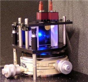
 This is the prototype measurement station that is capable of measuring five chips at a time
MEMS, or “MicroElectroMechanicalSystems” – deals with tiny circuits that are etched by the thousand on silicon wafers. They are used in mobile telephones, microphones and cars, foe example in sensors in airbags and tyres.
At present, inspecting these systems is a production bottleneck because they must be tested one at a time, which is a time-consuming and expensive process.
Parallel inspection
The EU's SMARTIEHS (SMART InspEction systems for High Speed and multifunctional testing of MEMS and MOEMS) is developing a new test concept based on parallel inspection of these circuits at wafer level. Testing a hundred units at once reduces the time required from 20 minutes to less than 30 seconds. Not only is this cheaper, but several more functions can be tested simultaneously.
SINTEF is coordinating this project, in which eight European micro-optics heavyweights are participating. They are now at the halfway point in the project.
“It was the industry itself that was looking for better and cheaper methods,” says Kay Gastinger of SINTEF ICT, who is coordinating the project.
“Today, tyre pressure sensors are only electrically tested during production, and theses tests do not guarantee full functionality. The research being performed by SMARTIEHS will mean cheaper sensors and more reliable equipment.
Detects deformations and faults
The research team uses an array of interferometers that can identify an object's shape, changes in shape and vibration extremely accurately. Standard microprocessor techniques are used to manufactures interferometers, making them cost-effective.
The underlying idea of the project is to produce a specially designed glass wafer that contains as many as 100 interferometers and then use this last to test 100 circuits on a MEMS wafer at one go. The scientists will be able to measure the shape, deformation and resonant frequency of the MEMS chips and thus identify manufacturing faults.
“We have already produced a prototype measurement station that is capable of measuring five chips at a time,” says Gastinger. The prototype consists of three wafers; the lens wafer, mirror wafer and beam-splitter wafer. The top layer contains 25 tiny lenses, which in principle resemble little microscopes and have an imaging function. Micromirrors at the centre of the lenses produce the interference effect.
The research teams are currently at the halfway stage in the project, which will come to an end in 2011, by which time the demonstrator will have been expanded to 50 channels, and the design will enable this number to be easily increased to 100.