Dec 9 2009
Nanoscale lithographic apparatus are indispensible tools used to manufacture integrated circuits (ICs), flat panel displays, optoelectronic and photonic devices as well as micro-electromechanical systems (MEMS), all involving nanoscale structures. The advancement in photolithography technology has been the key to the rapid development of the semiconductor industry. Countless innovations and progress in this field will continue to drive technological development in the semiconductor industry. Nanofabrication equipment has been used to create integrated circuits in the 65nm to 45nm range, and companies are now moving to manufacturing computer chips and memory chips in the 32nm range.
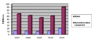
 share of Nanofabrication Equipment and wafers for Semiconductors, 2009-2014
According to a recently published report from iRAP, Inc., ET-110 Nanolithography Equipment for IT, Electronics and Photonics – A Technology, Industry and Global Market Analysis, the overall market for wafers and nanofabrication equipment is expected to grow at 11% a year for the next five years, from an estimated $65.8 billion in 2009 to $111 billion in 2014.
In 2008, nanofabrication apparatus enabled semiconductor manufacturers to transform more than $11.4 billion worth of silicon wafer material into more than $425 billion worth of semiconductor, photonic, opto-electonic and MEMS material devices for use in computers and electronic devices, which in turn constituted a global market valued in excess of $1.38 trillion dollars, plus related services valued at $5 trillion dollars globally. Semiconductor and electronics manufacturers spent roughly $80 billion in 2007 and $74 billion in 2008 for silicon wafers, materials and equipment which allowed them to manufacture integrated circuits at scales to 45nm, and they are now beginning to buy equipment to manufacture integrated circuits at the scales of 32nm and 22nm.
The equipment for deposition of materials onto silicon wafers represented 19% of the nanofabrication market and was valued at $11.4 billion for 2008. Lithographic equipment was 20% of the market, valued at $12.4 billion. Beam technology and light sources associated with lithography and semiconductors represented 9% of the market and were valued at $5.594 billion. Testing of semiconductor components and processes represented 17% of the nanofabrication market with a value of $10.56 billion. Metrology was 11% of the 2008 market, with a value of $6.83 billion. Other processes were 6% of the 2008 market, with a value of $3.730 billion.
Companies involved in nanofabrication materials, apparatus, metrology and testing for the IT and electronics industry had sales in excess of $80 billion in 2007 and more than $73.5 billion in 2008, reflecting the worldwide economic downturn. Research and development (R&D) spending for improved nanofabrication techniques and equipment exceeds $7 billion a year at the corporate level. Research and development of manufacturing equipment for 45nm technology for semiconductors, which began in 2003, is now the manufacturing standard, and the new standard under development is 32nm architecture, beginning to be implemented in 2009. Each reduction in size results in more powerful microprocessors, memory chips and silicon-based solar power collectors, in which creates new demands. Lithography, including masks and resist, and associated metrology currently comprises 30% to 40% of the entire cost of semiconductor manufacturing. This fraction depends strongly on the product mix, volume of integrated circuits in demand per design, and age of equipment in the factory.