Jan 6 2010
Computers keep getting more powerful because silicon transistors keep getting smaller. But that miniaturization can't continue much further without a change to the transistors' design, which has remained more or less the same for 40 years.
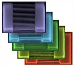
 Five different test structures feature stacks of nanowires with different numbers of levels. The bottom structure has only one level; the top structure has five. Images: Judy Hoyt, Pouya Hashemi and Leonardo Gomez
One potential successor to today's silicon transistors is silicon nanowires, tiny filaments of silicon suspended like the strings of a guitar between electrically conducting pads. But while silicon nanowires are certainly small enough to keep the miniaturization of computer circuitry on track, there's been doubt about whether they can pass enough electrical current for high-speed computing. At 2008's International Electron Device Meeting, researchers at MIT's Microsystems Technology Laboratories demonstrated silicon nanowires with twice the electron mobility — which indicates how easily current can be induced — of their predecessors. Now, the same group has shown that they can build chips in which up to five high-performance nanowires are stacked on top of each other. That would allow nanowire transistors to pass up to five times as much current without taking up any more area on the surface on the chip, a crucial step toward establishing the viability of silicon-nanowire transistors.
A transistor is basically a switch: when it's on, it passes an electrical current, and when it's off, it doesn't. Flipping the switch requires charging a part of the transistor called the “gate.” In today's design, the gate sits on top of the transistor. But if the transistor gets small enough, electricity will leak across it whether the gate is charged or not. Turning the switch off becomes impossible.
Because silicon nanowires are suspended in air, the gate can be wrapped all the way around them, like insulation around an electrical wire, which improves control of the switch. But the narrowness of the nanowires limits the amount of current they can pass.
Electrical-engineering professor Judy Hoyt and her graduate students Pouya Hashemi and Leonardo Gomez improved the performance of silicon-nanowire transistors by, basically, prying the atoms of the silicon slightly farther apart than they would be naturally, which allows electrons to flow through the wires more freely. Such “strained silicon” has been a standard way to improve the performance of conventional transistors since 2003. But Hoyt was one of the early researchers in the field.
“Starting in the early 1990s, she's really played a pioneering role in strained-silicon technology,” says Tahir Ghani, director of transistor technology and integration for Intel's Technology and Manufacturing Group. “She did a lot of this pioneering work that for the first time demonstrated that you can have significant performance gains by implementing strain into silicon technology.” Hoyt and her group's work on strained-silicon nanowires, Ghani says, “combines the two key elements of transistors” — performance and space efficiency — “both of which are very key to scaling in the future. And so from that standpoint, it makes it very relevant for industry.”
Handling stress
To build their stacked nanowire transistors, the MIT researchers begin with a normal silicon wafer, on which they deposit a silicon-germanium composite. Because germanium atoms are bigger than silicon atoms, the distances between atoms in the silicon-germanium layer are greater than they would be in a layer of pure silicon. When the researchers deposit another layer of silicon on top of the composite, the silicon atoms try to align themselves with the atoms beneath them, so they, too, end up spaced slightly farther apart.
This layer of strained silicon is bound to a second silicon wafer, and the other layers are removed, leaving the second wafer covered with a base layer of strained silicon. The researchers then stack alternating layers of silicon-germanium and silicon on top of the base layer, passing its strain on to each successive layer of silicon. Using a technique called electron-beam lithography, the researchers pattern fine lines onto the stacks and then etch away the material between the lines. Finally, they etch away the remaining silicon-germanium, and they're left with several layers of suspended silicon nanowires. Hoyt and her students have manufactured nanowires with a diameter of only eight nanometers, which they described in a 2009 paper in the Institute of Electrical and Electronics Engineers journal Electron Device Letters; by contrast, the smallest elements of today's computer chips are 45 nanometers across.
Hoyt says that her group can create silicon with two times the strain seen in chips built by commercial vendors. “We increase the germanium fraction of the initial layer, so we therefore build more stress into the silicon,” Hoyt says. Moreover, says Hashemi, “we are the only group in the world that has showed that we can maintain this strain after suspension” — that is, once the underlying layers have been cut away.
So far, Hoyt's group has built nanowire transistors in which charge is carried by moving electrons. But to maximize computational efficiency, a standard computer chip in fact uses two types of transistors. In the other type, charge is carried by so-called holes. A hole is simply the absence of an electron in a crystal of semiconducting material. When an electron slides over to fill the hole, it vacates its own spot in the crystal; another electron slides over to fill that spot; and so on. In this way, the hole in effect moves along the length of the crystal.
Increasing the mobility of holes in such transistors requires a different type of strain: the atoms of the crystal actually have to be jammed closer together than is comfortable. So Hoyt's group is now working to build nanowires from a silicon-germanium composite, where intervening layers of pure silicon cause compression rather than tension.