May 7 2010
BT Imaging Pty Ltd (BTi), the world's leading supplier of luminescence-based inspection and quality control systems for the photovoltaic manufacturing industry, today announced a breakthrough product for qualifying the electrical quality of as-cut wafers in production.
The QS-W1, the industry's first automated electrical wafer quality sorter, enables photovoltaic manufacturers to sort and reject as-cut wafers based on photovoltaic performance and maximize solar cell yield and efficiency. Utilizing BTi's proprietary second-generation patented photoluminescence (PL) imaging technology, the QS-W1 is ten times faster than previous generation systems, enabling inspection at production speeds for the first time. Initially targeting as-cut multi-crystalline silicon photovoltaic wafers, BTi has a roadmap in place to address the needs of mono-crystalline wafers and all photovoltaic cells at various stages of production. The QS-W1 is currently in extensive testing with leading photovoltaic wafer and cell makers.
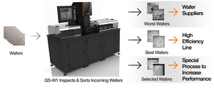
 BT Imaging's QS-W1 automatically sorts and qualifies photovoltaic wafers
"Our customers struggle with shrinking margins and controlling manufacturing cost," stated Ian Maxwell, chief executive officer of BT Imaging. "The QS-W1 benefits both wafer and cell manufacturers. Wafer manufacturers now have a solution to differentiate themselves based on superior electrical wafer quality. Cell makers can better predict cell efficiency and increase factory financial performance. We look forward to working with our customers to improve their electrical wafer and cell quality and to develop new and value-added applications for the QS-W1."
Photovoltaic solar cells are sold based on dollars per watt. Ideally, all solar cells would have maximum efficiency and revenue would be predictable. Today, however, there is a spread in processed cell efficiencies. Wafers are the largest cost element in solar cell manufacturing and can reduce absolute efficiency of a processed solar cell by as much as one percent. However, wafer electrical quality is not monitored today, and wafers are purchased at the same price based on physical specifications, regardless of final cell efficiency. Currently, wafers are checked at the end of the wafer manufacturing line for physical attributes like size, thickness, thickness variation, cracks, and roughness. Electrical defects such as dislocations and impurities -- which significantly impact cell electrical performance -- are not seen by current inspection techniques. These electrical defects remain in the cell and reduce the cell's performance. Cell electrical performance is determined only at the end of the cell process, in the IV tester; this final sorting is mandatory due to the inherent spread of wafer quality. At this stage, all wafers -- even the bad ones -- have been processed, so cell manufacturers have no means to further optimize yield and profits.
Inspection and Sorting at Production Speeds
Using BT Imaging's second-generation PL imaging technology, the QS-W1 is able to inspect as-cut wafers at production speeds. Ten times faster than the company's previous generation PL imaging technology, the QS-W1 can take high-resolution (1 MP) PL images of as-cut wafers in one second. Automated algorithms classify and report the different electrical defect types seen in as-cut silicon wafers. Defects that reduce efficiency and yield -- such as dislocations, impurities, and cracks -- are automatically separated and reported. User controlled binning is then used to grade the wafers appropriately based on defect density. The QS-W1 includes a crack and chip inspector and an integrated thickness and resistivity measurement unit, which is used to normalize PL data to ensure accurate grading and sorting. Fully automated, the base-model QS-W1 includes a coin stack loader that accommodates up to two load stations, fully integrated conveyor belt, input and output reject stations, and a coin stack sorter with six stations. Various handling options are available to meet specific customer needs.
Differentiate Wafer Quality
Wafer manufacturers can use the QS-W1 to differentiate their wafer quality and value by demonstrating with clear metrics the electrical entitlement of their wafers. In doing so, they can charge a premium for their wafers.
Increase Cell Line Electrical Performance
With the QS-W1, it is possible to inspect all wafers incoming to the cell line and sort based on electrical quality or reject wafers below a user defined electrical quality specification. In this way, wafers can be rejected before the cell processing cost is spent. This sorting of wafers enables cell makers to increase the cell conversion efficiencies and electrical yield of the line. The best wafers can be processed into high efficiency cells, poor quality wafers are rejected to wafer suppliers, and wafers with certain types of defects can go through extra processing to improve quality.
The QS-W1 will start shipping to beta customers in the third quarter of 2010. BT Imaging is accepting orders now. The QS-W1 will be on display at BT Imaging's booth -- Number T6068, Hall W6 -- at SNEC PV 2010 in Shanghai from May 5 through May 7, 2010. For more information, or to request a demo, please contact Wayne McMillan, vice president of sales and marketing.
Source: http://www.btimaging.com/