Oct 19 2010
There is a large growth market for flexible circuits, RFID antennas and biosensors on films. Researchers from the Fraunhofer Institute for Surface Engineering and Thin Films IST are presenting a new technology at K 2010, the international trade fair for plastics and rubber (Hall 3, E91): the experts can now apply conductive metal circuits to plastic substrates in a process that is energy- and material-conserving and thus more sustainable.
Flexible circuits can be found in many devices where space and weight considerations are dominant in the design of electronics: in cars, in cameras and video equipment, in mini-computers for athletes or in inkjet printers. And the market continues to grow: according to the business consultancy Frost & Sullivan, sales in this area will grow to more than $16 billion by the year 2014.
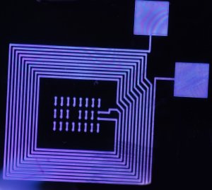
 Patterns like this one can be created on flexible films with the aid of plasma printing. Shown here: an RFID structure. (© Fraunhofer IST)
At K 2010, the trade fair for plastics in Düsseldorf, Germany, scientists from the IST in Braunschweig will unveil a new reel-to-reel technology for the production of flexible circuits and biosensors; the new technology is known as »P3T«, which is shorthand for »Plasma Printing and Packaging Technology«. The benefits: P3T involves considerably fewer process steps than existing processes, and it conserves raw materials. Unlike previous methods, the researchers do not start with a polymer film metalized over its entire surface from which excess metal is then removed to create the circuits. Instead, to produce flexible circuit boards, they apply circuits made of copper to the film that serves as substrate. In the case of biosensors, palladium is used. They use plasma at atmospheric pressure and galvanization instead of vacuum-pressure and laser-based methods to achieve inexpensive and resource-efficient production.
Dr. Michael Thomas, director of the research group at IST, explains: »During production of circuits for an RFID antenna, you often have to etch away between 50 and 80 percent of the copper used. This results in considerable amounts of copper scrap that either has to be disposed or reprocessed using relatively elaborate methods.« The IST approach is different: there, scientists use the additive process to apply the structures they want directly to the substrate sheeting.
The first two process steps are plasma printing at atmospheric pressure and metallization using well-known galvanization methods. Plasma printing uses the kind of deeply engraved roller familiar from the area of conventional rotogravure printing. During the printing process, microplasms are electrically generated in the engraved recesses of the roller; these microplasms chemically alter the surface of the plastic substrate where the circuits are to be applied later in the process.
The process gas from which the plasma is created is usually a mixture of nitrogenous gases. As IST researcher Thomas emphasizes: »The chemical changes we need begin to form on the surface of the film; these changes ensure that the plastic can be wetted with water in these precise areas and will be metallizable using suitable plating baths. This means considerable savings of energy and material,« Thomas adds. And this is a decisive competitive factor: the prices for raw materials – for copper and palladium, for example – have risen by around 150 percent in the past three years.
In the joint P3T project sponsored by the German Federal Ministry of Education and Research (BMBF) P3T, researchers are currently working very hard to improve the individual processes involved in the manufacture of flexible circuit boards and biosensors. They are closely scrutinizing all of the P3T production steps – from plasma printing to assembly and coordinating all of the processes with one another in a production line.