A CIC nanoGUNE research team and Neaspec (Germany) team have created a tool that enables scientists to record infrared spectra using a thermal device at a resolution more than in the existing infrared spectroscopy.
The technique could be used to analyze the local chemical composition and configuration of polymer composite nanomaterials, minerals, semiconductor devices or biological tissue.
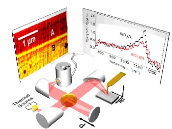
 NanoGUNE’s Infrared nanospectroscopy with a thermal source. The tip is illuminated with the broadband infrared radiation from of a thermal source and the backscattered
Infrared absorption determines a material’s chemical composition and structure. This is the reason behind the infrared spectrum being treated as the fingerprint of a material. Infrared spectroscopy helps characterize and recognize materials and is used in materials sciences and biomedical diagnostics. The light cannot focus dimensions less than several micrometers with optical systems such as FTIR (Fourier Transform Infrared) spectrometers. This constraint does not allow mapping of individual nanoparticles, molecules or semiconductor products.
The teams have designed an infrared spectrometer that enables nanoscale imaging using thermal radiation. The nano-FTIR is based on a scattering near-field microscope (NeaSNOM) deploying a sharp metallic probe to scan the topography of a surface. During the scanning process, the tip is lit with the infrared light emitted by a thermal device. The tip behaves like an antenna to alter the direct light into a nanoscale infrared spot or nanofocus at the tip. The scattered light was analyzed with a special FTIR spectrometer to enable recording of the infrared spectra emitted in nano volumes.
The infrared pictures of a semiconductor from Infineon Technologies (Munich) were recorded. A spatial resolution more than 100nm was attained. This revealed that thermal radiation could be targeted at a spot size hundred times tinier than the existing infrared spectroscopy, according to FlorianHuth. Nano-FTIR could help identify silicon oxides that have been differently processed or to determine the local electron density in complicated industrial electronic systems.
Nano-FTIR could be used in various sciences and technologies, including semiconductors, nanogeochemistry and astrophysics. It could also be used to map chemical composition and properties of organic and inorganic nano-systems, such as organic semiconductors, nanowires, ceramics, solar cells, and minerals.