FEI enhanced its ChemiSTEM Technology to facilitate energy dispersive X-ray (EDX) spectroscopy at the atomic level, which can be implemented for all the elements in the periodic table.
It is possible to obtain rapid results by increasing the current in an atom sized probe enabled by Cs adjustment, enhancing the sensitivity of X-ray detection and increasing the beam current This makes it ideal for materials science applications.
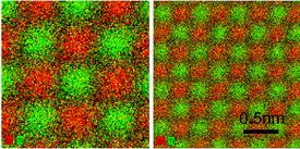
 The images show atomic-level EDX spectroscopy of the material Strontium Titanate; the individual atomic positions of the crystal structure can be easily distinguished by their chemical signal (red is Strontium, green is Titanium).
Professor Ferdinand Hofer of Graz University of Technology, Austria stated that the technology could be applicable in element-specific imaging at nano-resolution. A team at the university will use the technology to examine interfaces in LED’s, solar cell materials, ceramic materials and semiconductors.
George Scholes, vice president for product management at FEI said that the technology could enable groundbreaking results in important application areas such as microelectronics, catalysis, metallurgy, and green energy materials. Independent tests have shown that the core-shell structure comprising 5nm catalyst nanoparticles could be resolved in three minutes with high pixel resolution.
The use of this technology results in a factor of over 50 enhanced speed of EDX elemental mapping on transmission/ scanning electron microscopes (S/TEMs). The ChemiSTEM technology combines the X-FEG high brightness electron source, offering increased beam current at a specific spatial resolution, the patent-pending Super-X sensor system and fast scanning electronics, which enables accomplishing EDX spectral rates of 100,000 spectra per second. The windowless sensor design used in the four integrated SDD sensors has proved to ensure accurate detection of both light and heavy elements.