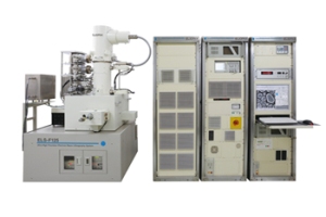
The Center for Nanoscale Systems (CNS) in Harvard has purchased the world’s first 125 kV electron beam lithography system, which is to be installed in the US.
This lithography system will be the most developed nanoscale patterning instrument. Researchers throughout the nation will have access to the Elionix ELS-F125 system by virtue of the participation of Harvard in the National Nanotechnology Infrastructure Network (NNIN) User Program of NSF.
 Elionix ELS-F125 Electron Beam Lithography System
The ELS-F125 is the Elionix’s latest addition to its range of electron beam lithography systems. This system has received the Nano-fabrication Technology Prize at Nano Tech in Japan, when the product was unveiled. Nano Tech has honored the Elionix ELS-F125 for its ability to consistently pattern 5 nm lines. The creation of the smallest line widths facilitates researchers to fabricate the devices and structures having advanced properties. These nano-devices have various applications in fields such as chemistry, electronics, optics and biology.
Besides having an acceleration voltage of 125 kV, the column design and electron optics of the Elionix system supplies high-beam currents and results in very high throughputs. Also, the Windows-based graphical user interface, which is newly designed, is well matched for the multi-user environment in Harvard’s Center for Nanoscale Systems.
Technical Director of Harvard’s Center for Nanoscale Systems, Dr. Eric Martin has stated that the ELS-F125 is offering user-friendly enhancements and enhanced throughput and the opportunity for consumers to produce outstanding results.