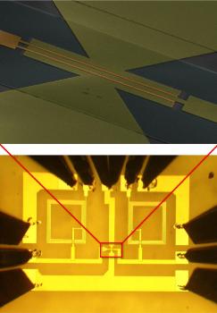
IBM researchers have developed an integrated circuit from wafer-size graphene, which operates as a broadband frequency mixer up to 10 GHz frequencies. This integrated circuit comprises a graphene transistor and an inductor pair integrated on a silicon carbide (SiC) wafer.
The complicated design challenges are met by using wafer-scale fabrication techniques that ensures the retention of graphene quality and enables integration to other devices in a complicated circuitry.
 Optical image of a completed graphene integrated circuit (IC) including contact pads
During the experiment, graphene is processed by thermal annealing of SiC wafers to develop even layers of graphene on the SiC surface. Graphene circuits are fabricated using four metal layers and two oxide layers to develop top-gated graphene transistor, interconnects, and on-chip inductors.
The circuit functions as a broadband frequency mixer, which generates output signals with mixed frequencies. Mixers are the basic units of most electronic communication systems. The graphene integrated circuit delivers good thermal stability up to 125°C.
The fabrication technique developed can be used with various kinds of graphene materials such as chemical vapour deposited (CVD) graphene films formed on metal films and works well with optical lithography for reduction in throughput and cost.
VP of Science and Technology, IBM Research, T.C. Chen, stated that with this innovation their scientists have accomplished a milestone in the nanotechnology field. He added that this innovation can result in an improvement in the performance of communication equipment, which will enable users to relate with each other more effectively. The research, funded by DARPA, is a major milestone achieved under the RF Applications (CERA) program.