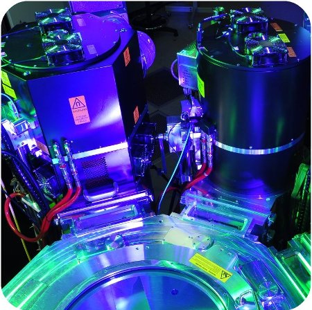
SPTS, the company that designs, manufactures and supplies etching solutions for the semiconductor industry, has launched the Pegasus Rapier module, which is a dry etch process tool for via reveal processes.
 Pegasus Rapier Module
The dry etch tool incorporates ReVia, the sole via reveal endpoint tool in the industry. The Pegasus Rapier tool has already been installed at top customer sites as the tool of record where it has been found to possess silicon etch rate twice as better than competitor products and etch uniformity of +/- 2.5% on bonded through silicon via (TSV) wafers of 300 mm diameter.
Subsequent to the formation of TSVs, the via reveal process is carried out. The wafer is attached to a carrier face down and the silicon surface is ground to a depth of 5 to 10 µm of the embedded TSVs. The vias filled with copper are revealed 5 µm high by subjecting the ground silicon surface to selective dry etching along the TSV liner oxide. Using dielectric, the via tips are passivated further after the dry etching. The copper is then exposed for redistribution layer metallization by polishing the via tips using chemical mechanical planarization. The total thickness variation (TTV) of the wafer is determined by the thickness of carrier wafer and TSV wafer, uniformity of TSV etch, bond layer and back grinding. TTV can lead to problems in ensuing process steps. The SPTS Pegasus Rapier module achieves best possible etch uniformity with 3 mm edge exclusion. It also features flexible multiple mode operation which allows for edge-fast etching to correct TTVs with issues.
Considerable time and money is spent in etching without endpoint reveal systems as the silicon thickness on every wafer above the TSV has to be measured due to the uncertainties characterizing silicon surface grinding, which necessitates the constant adjustment of etch time. The Pegasus Rapier facilitates the in-situ detection of the points at which the vias are revealed. The uniformity control, good etch rate and end point detection make the Pegasus Rapier module the perfect solution to deliver highest yield and low cost per die in high value wafer fabrication processes.