Apr 18 2013
Researchers are developing a new type of semiconductor technology for future computers and electronics based on "two-dimensional nanocrystals" layered in sheets less than a nanometer thick that could replace today's transistors.
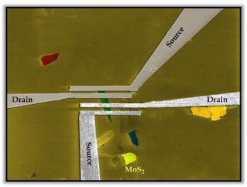
 Researchers are developing a new type of semiconductor technology, pictured here, for future computers and electronics based on "two-dimensional nanocrystals." The material is layered in sheets less than a nanometer thick that could replace today's silicon transistors. Credit: (Birck Nanotechnology Center, Purdue University)
The layered structure is made of a material called molybdenum disulfide, which belongs to a new class of semiconductors - metal di-chalogenides - emerging as potential candidates to replace today's technology, complementary metal oxide semiconductors, or CMOS.
New technologies will be needed to allow the semiconductor industry to continue advances in computer performance driven by the ability to create ever-smaller transistors. It is becoming increasingly difficult, however, to continue shrinking electronic devices made of conventional silicon-based semiconductors.
"We are going to reach the fundamental limits of silicon-based CMOS technology very soon, and that means novel materials must be found in order to continue scaling," said Saptarshi Das, who has completed a doctoral degree, working with Joerg Appenzeller, a professor of electrical and computer engineering and scientific director of nanoelectronics at Purdue's Birck Nanotechnology Center. "I don't think silicon can be replaced by a single material, but probably different materials will co-exist in a hybrid technology."
The nanocrystals are called two-dimensional because the materials can exist in the form of extremely thin sheets with a thickness of 0.7 nanometers, or roughly the width of three or four atoms. Findings show that the material performs best when formed into sheets of about 15 layers with a total thickness of 8-12 nanometers. The researchers also have developed a model to explain these experimental observations.
Findings are appearing this month as a cover story in the journal Rapid Research Letters. The paper was co-authored by Das and Appenzeller, who also have co-authored a paper to be presented during the annual Device Research Conference at the University of Notre Dame from June 23-26.
"Our model is generic and, therefore, is believed to be applicable to any two-dimensional layered system," Das said.
Molybdenum disulfide is promising in part because it possesses a bandgap, a trait that is needed to switch on and off, which is critical for digital transistors to store information in binary code.
Analyzing the material or integrating it into a circuit requires a metal contact. However, one factor limiting the ability to measure the electrical properties of a semiconductor is the electrical resistance in the contact. The researchers eliminated this contact resistance using a metal called scandium, allowing them to determine the true electronic properties of the layered device. Their results have been published in the January issue of the journal Nano
Letters with doctoral students Hong-Yan Chen and Ashish Verma Penumatcha as the other co-authors.
Transistors contain critical components called gates, which enable the devices to switch on and off and to direct the flow of electrical current. In today's chips, the length of these gates is about 14 nanometers, or billionths of a meter.
The semiconductor industry plans to reduce the gate length to 6 nanometers by 2020. However, further size reductions and boosts in speed are likely not possible using silicon, meaning new designs and materials will be needed to continue progress.