May 22 2013
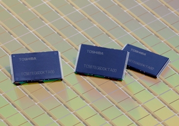
Toshiba America Electronic Components, Inc. (TAEC)*, a committed leader that collaborates with technology companies to create breakthrough designs, today announced that the company has developed second generation 19 nanometer process technology that it will apply to mass production of 2-bit-per-cell 64 gigabit NAND memory chips later this month.
 Toshiba NAND Flash Memory
Toshiba has used the new generation technology to develop the world's smallest * 2-bit -per-cell 64 gigabit NAND memory chips, with an area of only 94 square millimeters. Using a unique high speed writing method, the next generation chips can achieve a write speed of up to 25 megabytes a second - the world's fastest class * in 2-bit-per-cell chips.
Toshiba is also developing 3-bit-per-cell chips by using this process technology and aims to start mass production in the second quarter of this fiscal year. The company will initially introduce 3-bit, multi-level-cell products for smartphones and tablets by developing a controller compatible with eMMC, and will subsequently extend application to notebook PCs by developing a controller compliant with solid state drives (SSD).
NAND flash memory is an essential component of a diverse line-up of consumer products, including memory cards, smartphones, tablets and notebook PCs, and is increasingly deployed in enterprise products, including SSD for data centers. Looking to the future, Toshiba will continue to promote product innovation and development as a leading company in the market, able to respond to a wide variety of clients' needs.