Jun 28 2013
An LMU research team led by Bert Nickel has, for the first time, succeeded in functionally characterizing the active layer in organic thin-film solar cells using laser light for localized excitation of the material. The findings are reported in the scientific journal “Advanced Materials”.
 An LMU research team led by Bert Nickel has, for the first time, succeeded in functionally characterizing the active layer in organic thin-film solar cells using laser light for localized excitation of the material. The findings are reported in the scientific journal “Advanced Materials”.
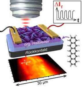
“We have developed a method in which the material is raster-scanned with a laser, while the focused beam is modulated in different ways, by means of a rotating attenuator for instance. This enables us to map directly the spatial distribution of defects in organic thin films, a feat which has not previously been achieved,” explains Christian Westermeier, who is first author of the new study.
Solar cells can convert sunlight into electrical power by exploiting light’s capacity to excite molecules, producing free electrons and positively charged “holes”. How long it takes for these charge carriers to be extracted by the electrodes is in turn dependent on the detailed structure of the cell’s active layer. Defects in the regular arrangement of the atoms act as temporary traps for charge carriers, and thus reduce the size of the usable current that can be produced. The new mapping method allows researchers to detect the changes in current flow associated with localized excitation of defects by laser light. In the utilized experimental geometry a metallic back contact serves as the gating electrode. By applying a voltage to this gate, the traps present in the semiconducting material can be filled or emptied in a controllable manner via the so-called field effect. By modulating the frequency of the laser light the temporal dynamics of trap states can be determined.
The study revealed that in pentacene, an organic semiconductor, the defects tend to be concentrated at certain positions. “It would be interesting to know what is special about the surface layer at these hot spots. What produces defects at these sites? They could be due to chemical contaminants or to irregularities in the alignment of the molecules,” says Bert Nickel, who is also a member of the Nanosystems Initiative Munich (NIM), a Cluster of Excellence.
Nickel and his colleagues chose the pentacene for their experiments because it is the most conductive material presently available for the manufacture of organic semiconductors. In the present study, they looked at a thin pentacene layer in which the majority of charge carriers are positively charged holes. In subsequent work, they plan to investigate complete solar cells, which consist of a hole-conducting film in direct contact with an electron-conducting layer.
(Advanced Materials, June 2013)