Oct 30 2013
Professor Angelika Kühnle and her work group at the Institute of Physical Chemistry at Johannes Gutenberg University Mainz (JGU) are participating in a new EU project focusing on information and communication technology. Over the next four years, a total of eight partners from six European countries will be involved in the "Planar Atomic and Molecular Scale Devices" (PAMS) project.
The goal is to manufacture planar electronic components to enable technological and scientific research to be conducted at the atomic or sub-molecular level. Kühnle's work group will receive some EUR 700,000 in funding under the 7th EU Research Framework Program.
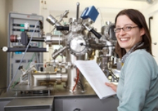
 Professor Dr. Angelika Kühnle. photo: Thomas Hartmann
The purpose of the PAMS project is to design electronic components that will be at a scale below the sub-nanometer range, in other words, in the atomic range. In order to do so, existing tools need to be further developed so that the necessary building blocks, such as nano wires and nano pads, can be connected and manipulated at low temperatures. Among the core aims of the research project is to understand the electronic functioning of these nano wires and the contacts between the various components for further improvement.
The Mainz-based team will focus on the synthesis of tailored molecular components. "We will be producing molecular structures on surfaces that, for example, will be used as molecular wires. The essential requirement is that these structures need to be directly synthesized on a non-conducting or semi-conducting carrier layer," explained Kühnle. "For this purpose, our cooperation partners will synthesize tailored precursor molecules with clearly defined properties." The precursor molecules will then be attached to isolating or semi-conducting surfaces under controlled conditions in an ultra-high vacuum environment. The next step will be to activate the precursor molecules on the surfaces by means of exposure to high temperatures or light irradiation. This should trigger a reaction that links the molecules, resulting in a stable, interlinked molecular component on the surface of the material.
Also participating in the EU project "Planar Atomic and Molecular Scale Devices" under supervision of Professor André Gourdon of the Centre National de la Recherche Scientifique (CNRS) in Toulouse, France, will be, in addition to Johannes Gutenberg University Mainz, the Jagiellonian University in Kraków, Poland, Dresden University of Technology, Germany, the University of Santiago de Compostela, Spain, the Spanish National Research Council in Madrid, Aalto University in Finland, and the IBM Research GmbH in Rüschlikon, Switzerland.