Nov 20 2013
A team of Clemson University physicists consisting of nanomaterial scientists Apparao Rao and Ramakrishna Podila and thermoelectricians Terry Tritt, Jian He and Pooja Puneet worked synergistically through the newly established Clemson Nanomaterials Center to develop a novel technique of tailoring thermoelectric properties of n-type bismuth telluride for high thermoelectric performance.
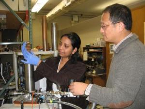
 Pooja Puneet, Ph.D., the lead author on the article published in Scientific Reports, and professor Jian He discuss their custom-made resistivity and Seebeck measurement system which is located in professor Terry Tritt's complex advanced material laboratory. Credit: Clemson University
Their findings were published in journal Scientific Reports.
The current US energy economy and environment are increasingly threatened by fast-dwindling domestic reserves of fossil fuel coupled with severe environmental impact of fossil fuel combustion. Highly-efficient thermoelectric devices are expected to provide clean energy technology-needs of the hour for US energy sustainability. This research is a step towards optimizing the device performance since it outlines a methodology to overcome a challenge that has "frustrated" thermoelectric researchers to date.
Thermoelectric (TE) devices convert waste heat into electricity through a unique material's property called the Seebeck effect. Basically, the Seebeck effect results in a voltage across the two ends of a TE material, akin to the voltage present across the two ends of a AA battery, when the TE material is properly exposed to the waste heat. In such devices, the efficiency of converting heat into electricity is governed by certain strongly coupled materials properties, viz., electrical resistivity, Seebeck coefficient, and thermal conductivity. A functional TE device consists of multiple legs made up of p-type and n-type materials, just as a diode comprises of a p-n junction.
Bismuth telluride (Bi2Te3) is a layered material and can be viewed as a deck of playing cards, wherein each card is only a few atoms thick. Bi2Te3 is currently regarded as the state-of-the-art TE material with high efficiency for converting waste heat into electricity, and is therefore attractive for energy harvesting processes.
Traditional nanosizing methods failed to improve the performance of n-type Bi2Te3 since they simply downgrade all materials properties simultaneously. Therefore, Clemson researchers and colleagues developed a novel nanosizing method in which we first peel n-type Bi2Te3 into atomically thin-sheets (akin to graphene which is one atom thick sheet of carbon atoms) and reassemble them using a spark plasma sintering process.
The researchers found that that the above described two-step process of first separating the deck of cards into individual cards and then re-assembling them into a deck via spark plasma sintering does enable us to suitably tailor the materials properties of n-type Bi2Te3for high TE performance. In this approach, the so-called 'interfacial charged defects' are generated in the sintered n-type Bi2Te3 which not only improves its structural properties but also its thermoelectric efficiency over a wide temperature window, thus making it extremely compatible with p-type Bi2Te3 for manufacturing efficient TE devices.
The improved compatibility factor (demonstrated in this paper) is expected to open new possibilities for highly efficient TE devices. The fascinating and noteworthy element of this research is that defects, which often connote impurity and are associated with low performance or efficiency, can indeed be used to tune the properties of materials to our advantage.
Today's scientific community lacks a comprehensive understanding of defects, mainly due to the absence of methods that can controllably generate and manipulate defects. The future of this research will be aimed at developing tools to generate and study defects at a fundamental level which will in turn allow the researchers to optimize materials properties of not only TE materials but also of a new class of two-dimensional materials beyond the Nobel-winning graphene for energy generation and storage.