Feb 14 2014
Researchers at the Helmholtz Center Berlin (HZB) have taken a leap forward towards a deeper understanding of an undesired effect in thin film solar cells based on amorphous silicon – one that has puzzled the scientific community for the last 40 years.
The researchers were able to demonstrate that tiny voids within the silicon network are partly responsible for reducing solar cell efficiency by some 10 to 15 percent as soon as you start using them. Their work has now been published in Physical Review Letters (DOI: 10.1103/PhysRevLett.112.066403).
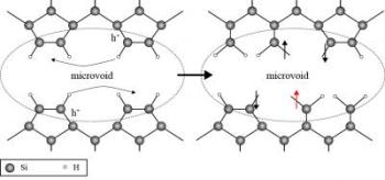
 In the initial state (left), the voids' internal surfaces are saturated with hydrogen atoms so that no defects are observed. Light-induced charge carriers (h+) destabilize atomic bonds. The breaking of atomic bonds causes defects (indicated by the vertical arrows on the right hand side), which translates to reduced solar cell efficiency. Credit: Picture: HZB
Amorphous silicon thin film solar cells are considered a promising alternative to solar cells based on highly purified silicon wafers, which have been dominating photovoltaic power generation. A major advantage of amorphous silicon thin film photovoltaics, where a glass substrate is coated with a light active material less than a thousandth of a millimeter thick, is that the cell fabrication is considerably simpler and much less costly than in the case of conventional crystalline silicon solar cells. On the other hand, a potential disadvantage is the low conversion efficiency from solar energy to electricity. Because of the disordered nature of amorphous silicon, solar cells are subject to the Staebler-Wronski effect, which reduces the solar cell efficiency by up to 15 percent within the first 1000 hours.
This undesired effect is triggered by internal annihilation – known in physics as recombination - of charge that has not been extracted from the solar cell. The released recombination energy induces defects in the amorphous network - which is why this effect is not observed in crystalline wafer solar cells. "However, where defects are produced in the material and whether voids of nanoscale size play a role in all this has not been understood – until now, that is," says HZB's own Matthias Fehr of the Institute for Silicon Photovoltaics. Fehr together with his HZB colleagues, scientists from Jülich Research Center and the Free University of Berlin have now made major strides towards unraveling this mystery.
Since the defects that form exhibit paramagnetic properties, they have a characteristic magnetic fingerprint, which depends on their microscopic environment. The Berlin researchers were able to identify this fingerprint using electron-paramagnetic resonance (EPR) spectroscopy and electron-spin echo (ESE) experiments. With the help of these highly sensitive techniques, they determined that defects in amorphous silicon actually come in two types: those that are uniformly distributed and those that are concentrated in clusters on internal surfaces of small voids - known in scientific circles as microvoids - which form within the material during the solar cell manufacturing process. "Our guess is that clusters of defects are generated on the internal walls of microvoids, which have a diameter of a mere one to two nanometers," explains HZB physicist Fehr. "Our findings seem to suggest that microvoids most likely contribute to light-induced degradation of amorphous silicon thin film solar cells. For us, it's been a leap forward towards a better understanding of the microscopic mechanism of light-induced degradation," says Fehr who, in 2013, spent a year conducting research in the US as a Feodor Lynen Scholar of the Alexander Humboldt Foundation. A new series of experiments has been designed to allow the Berlin researchers to glean further insights into the atomic and electronic processes of the Staebler-Wronski effect, named for the two scientists who first discovered it.
The work is part of the EPR-Solar network funded by the German Federal Ministry for Education and Research and the HZB's and FUB's Berlin Joint EPR Lab. According to the head of the project, Prof. Dr. Klaus Lips, "this is one of the major projects of one of the HZB's newest research departments, which is currently in the founding stage and whose mission is the fundamental physical characterization of energy materials with the goal of making an important contribution to the energy transition."