Apr 2 2014
Researchers in China, [J. Appl. Cryst. (2014). 47, 527-531] have found a convenient way to selectively prepare germanium sulfide nanostructures, including nanosheets and nanowires, that are more active than their bulk counterparts and could open the way to lower cost and safer optoelectronics, solar energy conversion and faster computer circuitry.
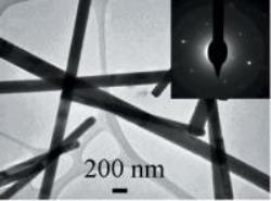
 This is a typical TEM image of as-prepared GeS nanowires with the inset showing a selected area electron diffraction pattern taken from GeS nanowires. Credit: Liang Shi and Yumei Dai
Germanium monosulfide, GeS, is emerging as one of the most important "IV–VI" semiconductor materials with potential in opto-electronics applications for telecommunications and computing, and as an absorber of light for use in solar energy conversion. One important property is its much lower toxicity and environmental impact when compared to other semiconductors made with cadmium, lead and mercury. It is less costly than other materials made with rare and noble metal elements. Indeed, glassy GeS has been used in lasers, fibre optic devices and infrared lenses as well as rewritable optical discs and non-volatile memory devices for several years. It is also used extensively as a solid electrolyte in conductive bridging random access memory (RAM) devices.
The repertoire of this material might be extended much further with the extra control that its use as nanostructured systems might allow. Liang Shi and Yumei Dai of the University of Science and Technology of China, in Hefei, point out that research in this area has lagged behind that with other IV-VI semiconductors. They hope to change that and have focused on how nanosheets and nanowires of GeS might be readily formed. They have used X-ray powder diffraction, transmission electron microscopy, energy-dispersive X-ray spectrometry and scanning electron microscopy to investigate the structure, morphology, composition and optical absorption properties of their samples.
The team used simple "wet" chemistry to synthesis their products using germanium dichloride-dioxane complex, thiourea and oleylamine (OLA) as starting materials. The ingredients were mixed in a sealed reaction flask, blasted with ultrasound to exclude air and then stirred and heated. The team was able to make nanosheets of GeS this way if the process was carried out for several hours at 593 Kelvin. At higher temperature, 613 Kelvin, they found that the sheets wind up into nanowires. Indeed, the precise heating time and temperature allowed them to control the structure of the final product. The team suggests that the rolling up of the nanosheets into nanowires is driven by the surface tension between the sheet and the OLA molecules during the heating.
Having proven the structural integrity of their GeS nanowires and nanosheets, the team built several test devices - a photoresponsive unit - which they used to evaluate the optical and electronic properties of the products. The team says that they have demonstrated "outstanding photoresponsive behaviour". This "indicates the potential use of as-synthesized GeS nanosheets and nanowires in solar energy conversion systems, such as the fabrication of photovoltaic devices".