Oct 8 2014
EV Group (EVG), a leading supplier of wafer bonding and lithography equipment for the MEMS, nanotechnology and semiconductor markets, today introduced the EVG®580 ComBond®―a high-vacuum wafer bonding system, which enables electrically conductive and oxide-free covalent bonds at room temperature.
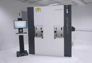
 The EVG(R)580 ComBond(R) automated high-vacuum wafer bonding system enables electrically conductive and oxide-free covalent bonds at room temperature. It is ideal for bonding materials with different properties to produce higher-performing electronic devices. (PRNewsFoto/EV Group (EVG))
Built on a modular platform to support high-volume manufacturing (HVM) requirements, the new system is ideally suited for bonding different substrate materials together in order to enable higher-performing devices and new applications, including:
- Multi-junction solar cells
- Silicon photonics
- High-vacuum MEMS packaging
- Power devices
- Compound semiconductor and other advanced engineered substrates for "beyond CMOS" applications such as high-mobility transistors, high-performance/low-power logic and radio frequency (RF) devices
Several EVG580 ComBond systems have already been shipped to device manufacturers and R&D centers. Customer demonstrations are available at EVG's corporate headquarters in St. Florian, Austria. Download the product datasheet at: http://www.evgroup.com/118694/118810/142472/EVG580_ComBond_ShortBrochure.pdf
"During the recent installation and acceptance test phase our new EVG580 ComBond has demonstrated its capacity to create excellent covalent bonds at room temperature. CEA-Leti is looking forward to working with EVG within our Common Lab on implementing the EVG580 ComBond to further development activities in several key areas," said Fabrice Geiger, VP Silicon Technologies Division at CEA-Leti.
"The EVG580 ComBond system masters the crucial surface preparation steps that are needed to ensure contamination- and oxide-free bonds at room temperature," stated Paul Lindner, executive technology director at EV Group. "With this breakthrough technology, we can bond nearly anything on anything—creating many different material combinations in wafer form. This supports our customers' efforts to develop and ramp new devices into mass production to enable a variety of emerging and high-growth applications—from the development of silicon photonics for next-generation telecommunications to more advanced power devices that can enable electric vehicles to drive longer distances between charges."
Challenges with Combining Compound Semiconductors and Silicon
Combining materials with different properties to produce electronic devices, such as III-V compound semiconductor materials like gallium nitride (GaN), gallium arsenide (GaAs) and indium phosphide (InP) with silicon substrates, can lead to enhanced device performance due to higher carrier mobility as well as open up new capabilities such as the emission of light through silicon, which can enable optical interconnects and routers. However, combining these materials through traditional epitaxial growth processes leads to crystal dislocation defects due to differences in lattice constant and coefficient of thermal expansion (CTE), which in turn degrade performance.
Benefits of Wafer Bonding
These manufacturing issues can be mitigated by growing each semiconductor material separately on optimized growth substrates and then combining them through wafer bonding. Room-temperature covalent bonding, in particular, is an ideal choice since it eliminates the need for annealing processes, which generate high temperatures that can add additional stress due to CTE mismatch. However, a key limitation of room-temperature covalent bonding has been the inability to maintain tight control of the thickness and uniformity of the bond interface layer, including effective removal of particle contaminants and the native oxide layers, which is necessary in order to achieve an interface that has both sufficient bond strength and electrical conductivity between the bonded materials. The EVG580 ComBond addresses these limitations.
Key EVG580 ComBond Features
- Dedicated ComBond Activation Module (CAM) seamlessly integrated into the platform, which provides advanced surface preparation by directing energized particles to the substrate surface instead of wet chemical etching to achieve a contamination-free and oxide-free bond interface
- Operates in a high-vacuum-process environment, which prevents re-oxidation of the treated wafers prior to the bonding step
- Configurable with up to five modules that can process in parallel to support both R&D and HVM applications
- Processes wafer sizes up to eight inches (200-mm)
EV Group and EVG580 ComBond at SEMICON Europa
Media and analysts interested in learning more about the company and its latest developments in covalent bonding and other applications at SEMICON Europa 2014, October 7-9, are invited to visit EVG's booth #918 in the ALPEXPO, Grenoble, France, as well as attend the company's presentations during the show's technical program. EVG representatives will present "Future of MEMS: Market and technologies perspective" at the International MEMS Industry Forum on October 7 from 09:50 to 10:10, "Hybrid wafer bonding for 3D IC" at the 3D Integration Session on October 8 from 15:40 to 16:00, and "Nanoimprint status for HVM" at the Lithography Session on October 9 from 13:10 to 13:30.