Mar 31 2016
In the world of nano-scale technology, where work is conducted at the atomic level, even the smallest changes can have an enormous impact. And a new discovery by a University of Alberta materials engineering researchers has caught the attention of electronics industry leaders looking for more efficient manufacturing processes.
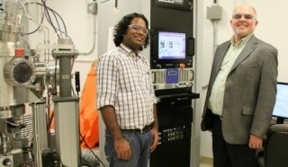
 UAlberta materials engineering postdoctoral fellow Triratna Muneshwar and materials engineering professor Ken Cadien have developed a new method of making thin films. Their research appears in the Journal of Applied Physics. (credit: UAlberta Engineering)
Triratna Muneshwar, a postdoctoral fellow in the Department of Chemical and Materials Engineering and Ken Cadien, a materials engineering professor, have developed a new method of making thin films—materials that are essential in today’s computers and electronic devices—by adapting current atomic layer deposition techniques.
Atomic layer deposition (ALD) is exactly what the name implies. Thin films are coated with molecule-thin layers of materials like zinc, silicon, nitrogen, and so on. In the manufacturing process, the film is placed inside a small chamber and prepared by being treated with a “sticky” precursor layer. Gasses are then pumped inside, coating and chemically binding to receptors on the precursor layer.
The problem is that some of the molecules coming to rest on top of the precursor layer are so large that they block other receptor points. It’s like five people taking up 10 seats on a bus.
However, Muneshwar observed that those large molecules almost immediately shed ligands that do not connect to the precursor layer, freeing up previously blocked receptors. But by this time, the gas has been pumped out of the chamber and cannot be used a second time.
“Although few strategies have been proposed to recycle this unreacted gas, residual impurities within remains a serious concern,” he notes.
Muneshwar wondered if he could create a more dense and uniform layer by pumping gas into the chamber in smaller doses, waiting just a fraction of a second for the ligands to slough off and free up receptors, and then pumping in another small dose of gas.
He developed the idea while working as a PhD under Cadien’s supervision.
“My interest in this came about in a conversation with Dr. Cadien and one of his colleagues who said that precursor costs are a challenge,” said Muneshwar. Then, while attending an international conference in last year, Muneshwar asked industry engineers and researchers about ALD and precursor costs in particular.
“I asked one fellow ‘What if I could cut your precursor costs in half?’ and he realized the impact this would have on their manufacturing processes. Later that day when I ran into him, I was told that he discussed this idea with his boss and they would be very interested in our work,” Muneshwar said.
After returning to campus, Muneshwar began crunching numbers and found that on paper, the pulsed layering concept held promise. After refining his work, Muneshwar had developed a mathematical model that demonstrated the technique would work.
“In a lot of cases you do an experiment and then come up with the formula that explains what happened,” Cadien said. “But Triratna wrote the model first and it predicted exactly what happened in the experiment.”
Muneshwar and Cadien have published a paper on their discovery in the Journal of Applied Physics. Since the article’s appearance, they have been contacted by industry leaders requesting copies of the paper.
While small amounts of materials like zinc or silicon are required to produce thin film devices, Cadien says the costs are not insignificant—they can come in at $500 or $600 per gram and the current processes are wasteful, dosing surfaces with anywhere from 100 to 10,000 times the molecules required.
“Some of these are big molecules and in semiconductor manufacturing if you’re a company producing 10,000 12-inch wafers a week—small amounts of something add up to big amounts of something.”
The market for devices manufactured using ALD is estimated to hit $400 million U.S. by 2020.
The two hope their discovery can lead to collaborative work with new industry partners in the future. Cadien notes that Muneshwar’s work could have a lasting impact on industrial practices because he was willing to experiment with the high-tech equipment available to him here.
“There are more than 1,000 atomic layer deposition systems in the world,” said Cadien, “but there’s only a small handful of people asking why and how these things work, who are trying new things. When you’re doing that, you can come up with breakthroughs like this.”