Apr 19 2016
Growing crystalline film layers, also known as epitaxy, are templated using a crystalline substrate. Epitaxy is considered to be the foundation to develop semiconductors and transistors. If the material in onr deposited layer is the same as the material present in the next layer, it energetically helps the formation of firm bonds between perfectly matched, highly arranged layers. In comparison to this, it is extremely difficult to even attempt to layer dissimilar materials when the crystal lattices fail to easily match. In this case, weak van der Waals forces develop attraction but do not develop firm bonds between unlike layers.
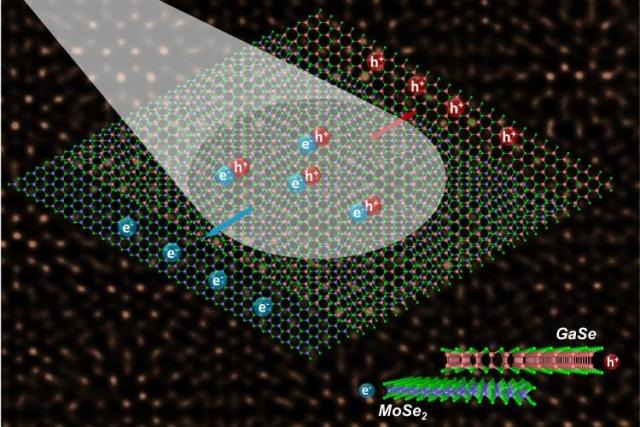
 Light drives the migration of charge carriers (electrons and holes) at the juncture between semiconductors with mismatched crystal lattices. These heterostructures hold promise for advancing optoelectronics and exploring new physics. The schematic’s background is a scanning transmission electron microscope image showing the bilayer in atomic-scale resolution. Image credit: Oak Ridge National Laboratory, U.S. Dept. of Energy. Image by Xufan Li and Chris Rouleau
The Department of Energy’s Oak Ridge National Laboratory led research where scientists synthesized a pile of atomically thin monolayers belonging to two lattice-mismatched semiconductors. One semiconductor is molybdenum diselenide, which is an “n-type” semiconductor with increasing volumes of electron charge carriers. The other semiconductor is gallium selenide, which is a “p-type” semiconductor known for its charge carriers referred to as “holes”. The semiconductor layers met at a point and developed an atomically sharp heterostructure, known as a p–n junction, which was capable of generating a photovoltaic response by segregating electron–hole pairs generated by light. Science Advances features a report explaining that the success of developing the atomically thin solar cell highlights the possibility of synthesizing mismatched layers to help new families of useful two-dimensional (2D) materials.
The concept of piling varied materials on top of each other has been in existence for quite a long time, and is now followed as a standard step for most of the top electronic devices currently in use. Generally, this kind of piling works only when the individual materials have extremely similar crystal lattices, or in other words a fine “lattice match.” This is the point where the current research explores a new territory by developing superior quality layers of a variety of 2D materials, increasing the number of materials that are capable of being combined, and thus forming a variety of potential atomically thin electronic devices.
Because the two layers had such a large lattice mismatch between them, it’s very unexpected that they would grow on each other in an orderly way, but it worked.
Xufan Li, Postdoctoral Research Associate, ORNL
For the very first time, the research group demonstrated that monolayers of two different kinds of metal chalcogenides, binary compounds of sulfur, tellurium or selenium with an enhanced electropositive radical or element, comprising of varied lattice constants are capable of being grown together to create an accurately positioned stacking bilayer.
It’s a new, potential building block for energy-efficient optoelectronics.
Xufan Li, Postdoctoral Research Associate, ORNL
The researchers characterized their new bilayer building block and discovered that both the mismatched layers self-assembled themselves into a repeating long-range atomic order that could be visualized directly by the Moiré patterns displayed in the electron microscope.
We were surprised that these patterns aligned perfectly.
Xufan Li, Postdoctoral Research Associate, ORNL
Researchers from David Geohegan’s ORNL Functional Hybrid Nanomaterials group executed a study along with partners at Beijing Computational Science Research Center, the University of Utah, and Vanderbilt University.
These new 2D mismatched layered heterostructures open the door to novel building blocks for optoelectronic applications. They can allow us to study new physics properties which cannot be discovered with other 2D heterostructures with matched lattices. They offer potential for a wide range of physical phenomena ranging from interfacial magnetism, superconductivity and Hofstadter’s butterfly effect.
Kai Xiao, Staff Scientist, ORNL
A monolayer of molybdenum diselenide was initially grown by Li, and this was then followed by growing a gallium selenide layer on top. This procedure, known as “van der Waals epitaxy,” refers to the weak attractive forces that have the potential to hold together dissimilar layers.
With van der Waals epitaxy, despite big lattice mismatches, you can still grow another layer on the first.
Xufan Li, Postdoctoral Research Associate, ORNL
The researchers used scanning transmission electron microscopy to characterize the atomic structure of the materials and then showed the formation of Moiré patterns.
In the future, the researchers plan to carry out studies exploring the alignment of materials during the growth process and also the influence of material composition on the properties beyond the photovoltaic response. Emphasis will be placed on incorporating 2D materials into devices.
Study on layering a variety of compounds with matching lattice cell sizes has been a popular research topic for many years. A wide range of elements have been added into the compounds to develop different physical properties corresponding to thermoelectrics, magnetism and superconductivity. However, layering 2D compounds with different lattice cell sizes is an unexplored territory.
We’ve opened the door to exploring all types of mismatched heterostructures.
Xufan Li, Postdoctoral Research Associate, ORNL
The title of the paper is “Two-dimensional GaSe/MoSe2 misfit bilayer heterojunctions by van der Waals epitaxy.”
The DOE Office of Science supported the research, including materials synthesis. Materials characterization was partially conducted at the Center for Nanophase Materials Sciences, a DOE Office of Science User Facility at ORNL. Some of the device measurements in the study were financially supported by ORNL Laboratory Directed Research and Development funds.