Jul 12 2016
Researchers at the U.S. Department of Energy’s Lawrence Berkeley National Laboratory (Berkeley Lab) have formulated a method to chemically build circuits and transistors that measure just a few atoms in thickness. This progress has the potential for advanced computing technologies and electronics - even paper-thin gadgets.
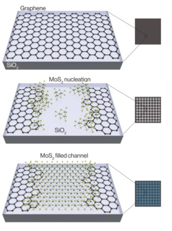
 This schematic shows the chemical assembly of two-dimensional crystals. Graphene is first etched into channels and the TMDC molybdenum disulfide (MoS2) begins to nucleate around the edges and within the channel. On the edges, MoS2 slightly overlaps on top of the graphene. Finally, further growth results in MoS2 completely filling the channels. (Photo credit: Berkeley Lab)
The method also provides functional structures at an adequately large scale, which could lead to commercial scalability and real-world applications. They published their research findings online in the Nature Nanotechnology journal.
The team managed to control the synthesis of a transistor where a semiconducting material referred to as a transition-metal dichalcogenide (TMDC) was seeded in the blank channels, and narrow channels were etched onto conducting graphene. Both of these materials are atomically thin and single-layered crystals, the two-part assembly produced electronic structures that are fundamentally 2D.
Also, the synthesis could cover an area measuring a few centimeters in length and a few millimeters width.
This is a big step toward a scalable and repeatable way to build atomically thin electronics or pack more computing power in a smaller area.
Xiang Zhang, Senior Scientist, Berkeley Lab
Zhang also holds the Ernest S. Kuh Endowed Chair at the University of California (UC) Berkeley and is a member of the Kavli Energy NanoSciences Institute at Berkeley. Other scientists who contributed to the research include Mervin Zhao, Yu Ye, Yang Xia, Hanyu Zhu, Siqi Wang, and Yuan Wang from UC Berkeley as well as Yimo Han and David Muller from Cornell University.
Their research falls into place with a new area of interest that aims to keep pace with Moore’s Law. The law proposes that the number of transistors in an integrated circuit doubles roughly every two years. To maintain this pace, scientists estimate that integrated electronics will quickly need transistors that measure under 10 nm in length.
Principally, transistors are electronic switches and must be able to switch on and off, which is a typical feature of semiconductors. However, at the nanometer scale, silicon transistors mostly will not be a good option. The reason for this is silicon is a bulk material, and when silicon-based electronics become smaller and smaller, their performance as switches significantly reduces, which is a major barrier for future electronics.
To maintain the pace prescribed by Moore’s Law, the team chose to work with 2D crystals that measure just one molecule in thickness. These crystals are not governed by the limitations of silicon.
Along these lines, the Berkeley Lab team created a method to seed a single-layered semiconductor - for this study TMDC molybdenum disulfide (MoS2) - into channels lithographically etched within a sheet of conducting graphene.
The two atomic sheets join to form junctions at nanometer scale that facilitate graphene to effectively inject current into the MoS2. It is these junctions that form atomically thin transistors.
This approach allows for the chemical assembly of electronic circuits, using two-dimensional materials, which show improved performance compared to using traditional metals to inject current into TMDCs.
Mervin Zhao, Ph.D. Student, Berkeley Lab
Electron and optical microscopy images, and spectroscopic mapping, validated numerous aspects related to the successful development and functionality of the 2D transistors.
Additionally, the researchers illustrated the structure’s applicability by assembling it into an inverter’s logic circuitry. This further highlights the ability of the technology to pave the way for a chemically assembled atomic computer, explained the researchers.
Both of these two-dimensional crystals have been synthesized in the wafer scale in a way that is compatible with current semiconductor manufacturing. By integrating our technique with other growth systems, it’s possible that future computing can be done completely with atomically thin crystals.
Mervin Zhao, Ph.D. Student, Berkeley Lab
The Office of Naval Research and the National Science Foundation supported this research.