Oct 4 2017
The Science
Researchers at the Center for Functional Nanomaterials (CFN) have been successful in carving structures at the single molecule level by using an ultra-modern electron microscope. The method enables achieving an unparalleled resolution of 1 nm.
The outcomes are a remarkable advancement over the largely applied nanofabrication method, that is, electron-beam lithography, through which minute details such as these cannot be accomplished.
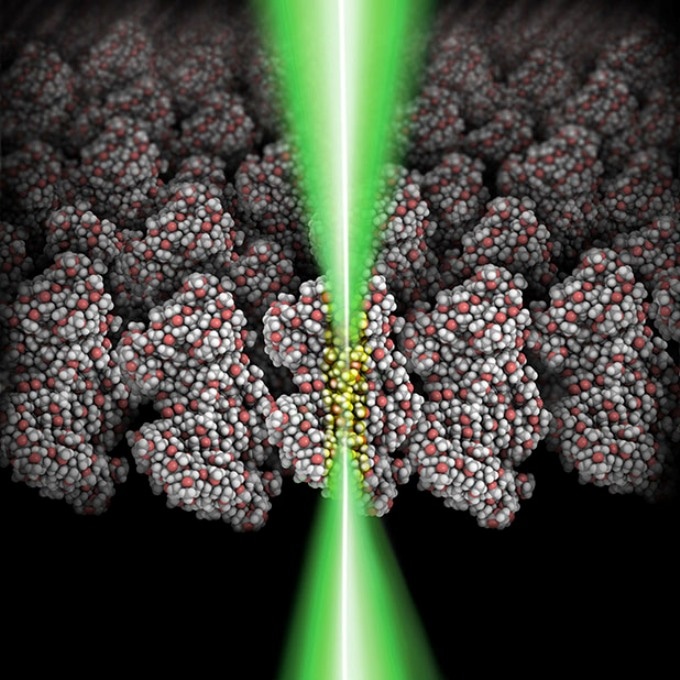
 A schematic showing a focused electron beam (green) shining through a polymeric film (grey: carbon atoms; red: oxygen atoms; white: hydrogen atoms). The glowing area (yellow) indicates the molecular volume chemically modified by the focused electron beam. CREDIT: Image courtesy of the Center for Functional Nanomaterials at Brookhaven National Laboratory.
The Impact
By applying CFN’s innovative technique, Researchers can now design individual molecules for developing a film that has distinctive characteristics. For instance, they will be able to develop films with the ability to more effectively conduct electricity. The method can be adopted by Researchers to create a wide range of innovative materials, structured with unpredictable shapes. Researchers can develop the materials with close-to-atomic-scale manipulation.
Summary
There has been much advancement in the field of nanotechnology due to the potential to design materials at extremely smaller sizes by adopting electron-beam lithography where a focused beam of electrons impacts on an electron-sensitive material.
By reducing the characteristic size of materials from the macroscale to the nanoscale, individual molecules and atoms can be controlled to drastically modify material characteristics, for example, electrical conductivity, light interactions, chemical reactivity and color.
In an endeavor to design materials that have extremely smaller characteristic sizes, Researchers from the CFN, which is a U.S. Department of Energy Office of Science user facility at Brookhaven National Laboratory, have created a new record in the recent past.
They have adopted electron-beam lithography carried out using an ultra-modern scanning transmission electron microscope to design thin films of the poly(methyl methacrylate) (PMMA) with individual characteristics as small as 1 nm, where the spacing between the features is 11 nm.
This yielded an areal density of close to 1 trillion features in 1 cm2 of the film. The PMMA films designed by the Researchers can be applied as stencils for conveying the drawn single-digit nanometer feature into any material. As part of the study, the Researchers developed structures smaller than 5 nm in both semiconducting (zinc oxide) and metallic (gold palladium) materials.
The size of the fabricated gold palladium alloy features was just 6 atoms wide. This method has paved the way for a number of exhilarating materials engineering probabilities, customizing characteristics at the atomic scale. The CFN will be shortly providing this state-of-the-art nanoscience tool to Researchers globally.