Oct 13 2017
An innovative study performed by Researchers from the Department of Energy’s Lawrence Berkeley National Laboratory (Berkeley Lab) has shown that the electrostatic charge that makes hair stand on end and attaches balloons to clothing can be efficiently used to drive futuristic atomically thin electronic memory devices.
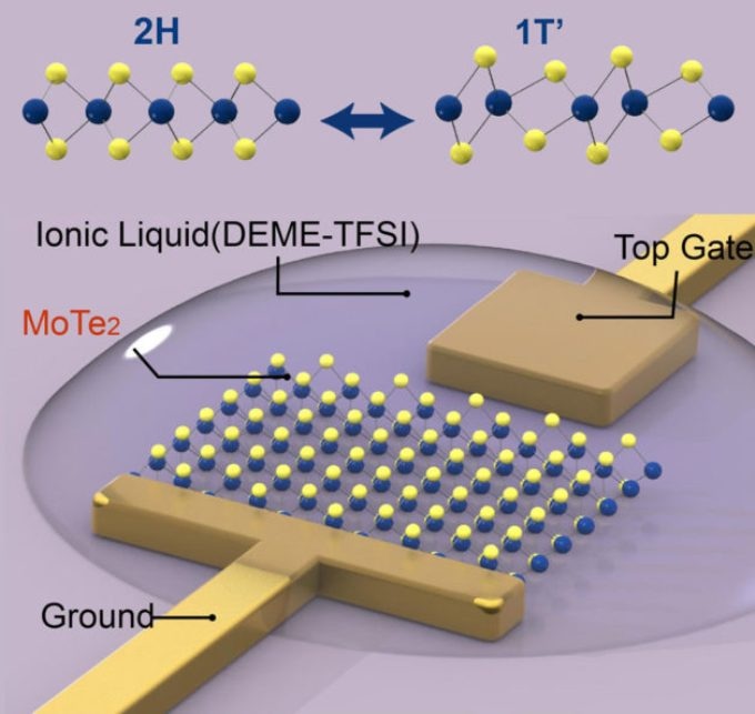
 Schematic shows the configuration for structural phase transition on a molybdenum ditelluride monolayer (MoTe2, shown as yellow and blue spheres), which is anchored by a metal electrodes (top gate and ground). The ionic liquid covering the monolayer and electrodes enables a high density of electrons to populate the monolayer, leading to changes in the structural lattice from a hexagonal (2H) to monoclinic (1T’) pattern. CREDIT: Ying Wang/Berkeley Lab.
In a research reported in the Nature journal on October 11th, 2017, Researchers have discovered a technique to reversibly alter a 2D material’s atomic structure by injecting, that is, “doping,” electrons into the material. The technique uses considerably less energy when compared to other prevalent techniques for modifying the layout of the structure of a material.
We show, for the first time, that it is possible to inject electrons to drive structural phase changes in materials. By adding electrons into a material, the overall energy goes up and will tip off the balance, resulting in the atomic structure rearranging to a new pattern that is more stable. Such electron doping-driven structural phase transitions at the 2-D limit is not only important in fundamental physics; it also opens the door for new electronic memory and low-power switching in the next generation of ultra-thin devices.
Xiang Zhang, Principal Investigator of the study, Senior Faculty Scientist Materials Sciences Division, Berkeley Lab and a Professor at UC Berkeley
Modifying the structural layout of a material from one phase to another is the basic, binary feature in prevalent digital circuitry. The size of electronic components powered with the ability of such phase transition has been considerably reduced to paper-thin form. However, even today, Scientists consider them to be bulk, 3D layers. In contrast, 2D monolayer materials are formed of a single layer of molecules or atoms with a thickness that is 100,000 times smaller than that of human hair.
“The idea of electron doping to alter a material’s atomic structure is unique to 2-D materials, which are much more electrically tunable compared with 3-D bulk materials,” stated Jun Xiao, Co-lead Author of the study, who is a graduate student in Zhang’s lab.
The standard technique for enabling structural transition of materials involves heating to more than 500°C. Techniques such as this consume large amounts of energy and cannot be applied for practical applications. Moreover, the surplus heat can considerably decrease the service life of integrated circuit components.
Many research teams have analyzed the use of chemicals to modify the structural layout of atoms in semiconductor materials. However, this process is tough to control to date and has not been largely used for industrial application.
Here we use electrostatic doping to control the atomic configuration of a two-dimensional material. Compared to the use of chemicals, our method is reversible and free of impurities. It has greater potential for integration into the manufacturing of cell phones, computers, and other electronic devices.
Ying Wang, Co-lead Author of the study
The team coated molybdenum ditelluride (MoTe2)—a classic 2D semiconductor—with an ionic liquid (DEME-TFSI) having an ultra-high capacitance, that is, the potential to store electric charges. The ionic liquid layer enabled the team to dope the semiconductor with electrons at a density of one hundred trillion to a quadrillion for one square centimeter of the semiconductor. According to the Researchers, the magnitude of this electron density is one to two orders higher than that accomplished in 3D bulk materials.
The team adopted spectroscopic analysis and elucidated that doping with electrons modified the configuration of the molybdenum ditelluride atoms from a hexagonal shape to a monoclinic form (i.e. slanted cuboid shape). Upon retracting the electrons, the crystal structure was found to be reversed to its original hexagonal pattern, indicating that the phase transition can be reversed. Furthermore, the symmetries of the two types of atom arrangements are considerably different, ensuring a large divergence for usage in optical components.
Such an atomically thin device could have dual functions, serving simultaneously as optical or electrical transistors, and hence broaden the functionalities of the electronics used in our daily lives.
Ying Wang, Co-lead Author of the study
DOE’s Office of Science and the National Science Foundation supported the research.