Jan 24 2018
Physicists have devised a new, optical microscopy-based method that can be used for creating images of nanoscale atoms. The novel technique makes it possible to image quantum dots in a semiconductor chip. Along with coworkers from the University of Bochum, researchers from the Swiss Nanoscience Institute and the University of Basel’s Department of Physics reported their findings in the journal, Nature Photonics.
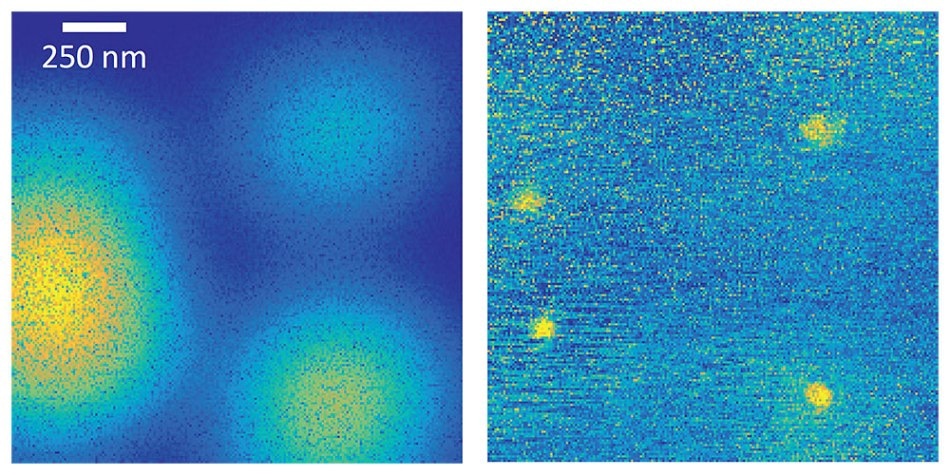
 An image of quantum dots in a semiconductor (right), versus the image taken with a normal microscope (left). The new method clearly shows four quantum dots (bright yellow spots). (Image credit: University of Basel, Department of Physics)
Microscopes enable humans to visualize structures that otherwise cannot be seen by the naked eye. However, individual atoms and molecules, which measure only a few nanometers across, cannot be imaged with traditional optical microscopes. This is attributed to the wave nature of light and the related laws of physics, which were developed by the German physicist Ernst Abbe in 1873.
According to these laws of physics, the maximum resolution of a microscope is equivalent to half the wavelength of the light utilized. For instance, if green light with a wavelength of 500 nanometers is used, an optical microscope would be best able to differentiate objects at a distance of 250 nanometers.
Switched On and Off
However, in the past few years, researchers have effectively managed to get around this resolution limit and create images of structures that measure just fractions of a nanometer across. In order to achieve this, they utilized lasers of different wavelengths to activate fluorescence in molecules in part of the substance and at the same time suppressed it in the surrounding areas. This technique enables them to image structures, for example dye molecules, which measure only a few nanometers in size. The development of this innovative technique (Stimulated Emission Depletion, STED) received the Nobel Prize in Chemistry earlier in 2014.
For All Objects With Two Energy Levels
Timo Kaldewey, from Professor Richard Warburton’s team at the University of Basel’s Department of Physics and Swiss Nanoscience Institute, has now worked with coworkers at Ruhr-University Bochum (Germany) in order to devise a similar method that makes it possible to image objects on the nanoscale objects, especially a quantum mechanical two-level system.
The physicists examined the so-called quantum dots – artificial atoms in a semiconductor – which were successfully imaged as bright spots using the new method. The researchers then excited the atoms with a pulsed laser, which alters its color during each pulse. Consequently, the fluorescence of the atom is switched on and off.
While the STED technique only functions by occupying a minimum of four different energy levels in response to the laser excitation, Basel’s method also works with atoms that have only two energy states. These kinds of two-state system constitute significant model systems for quantum mechanics.
The new technique is different from STED microscopy and does not emit any heat. “This is a huge advantage, as any heat released can destroy the molecules you’re examining,” explains Richard Warburton. “Our nanoscope is suitable for all objects with two energy levels, such as real atoms, cold molecules, quantum dots, or color centers.”
Among other sources, the National Center of Competence in Research “Quantum Science and Technology” (NCCR QSIT), the Swiss National Science Foundation, and the European Union under the FP7 program funded the project.