May 1 2018
Researchers from the Penn State and Southwest Jiaotong University and Tsinghua University in China have developed a precise, chemical-free technique for etching nanoscale features on silicon wafers.
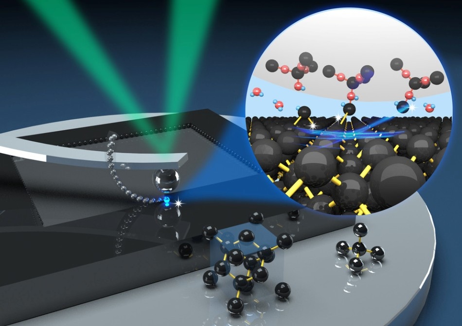
 A single layer of silicon atoms (black) bind to the moving silica tip of a scanning probe microscope. (Image credit: Lei Chen/Southwest Jiaotong University)
In typical lithography, a photosensitive film is placed on a silicon wafer and a pattern known as a mask is used to expose some portions of the film. Then, chemicals—such as a potassium hydroxide solution—are used to etch patterns into the silicon. More steps are necessary to smooth out the coarse surface.
The Penn State and Southwest Jiaotong University scientists created a completely different, chemical- and mask-free, one-step process. They mildly rubbed a rounded silica tip of an instrument known as a scanning probe microscope across a silicon substrate—the material base usually used to manufacture electronic devices. When exposed to the water vapor in air, the top layer of silicon develops bonds with the tip of the scanning probe, and a single layer of atoms slides off as the probe travels across the silicon. As the atoms below do not join the chemical reaction, they are totally undamaged.
It's really quite a unique idea. It's a so-called tribochemical reaction. Unlike chemical reactions caused by heat, light or electric fields, which are all widely studied, mechanically-stimulated chemical reactions are less understood.
Seong Kim, Professor of Chemical Engineering - Penn State
The removal mechanism is started when the silicon is exposed to air and the top atomic layer of silicon atoms reacts with water molecules to create silicon-oxygen-hydrogen bonds. Then the silicon oxide surface of the tip develops a silicon-oxide-silicon bond with the substrate surface because of the shear force of the moving tip. This assists the removal of the silicon atom from the substrate’s topmost surface.
People interested in nanofabrication who are attempting to decrease the size of device features down to atomic-scale dimensions may find this method useful, Kim believes.
"Atomic layer etching can provide the depth resolution that people would like to get without the use of sacrificial layers and harsh chemicals," he said.
This sort of patterning technique is extremely slow for microfabrication at present, Kim acknowledged. However, scientists could use it to develop a platform for testing electronic and microelectromechanical devices with properties at the Angstrom or single-atom scale, much smaller than current devices. At least one company, IBM, has tested with multiple probe arrays that could pave the way for large-scale patterning of devices.
Our process could be combined with their process to scale up. This is the initial science part. Once we see the science, a lot of possibilities can be explored. For instance, we think this technique will work with other materials beyond silicon.
Seong Kim, Professor of Chemical Engineering - Penn State
The scientists explain their method in Nature Communications in an article titled "Nanomanufacturing of Silicon Surface with a Single Atomic Layer Precision via Mechanochemical Reactions."
The first and second authors, Lei Chen and Jialin Wen, were visiting scholars at Penn State and continued working with Kim on tribochemical reactions when they went back to China. Kim's long-time collaborator, Linmao Qian of Southwest Jiaotong University, is co-corresponding author together with Kim.
The U.S. National Science Foundation, the National Science Foundation of China, and the Science Challenge Program of China supported this research.