Dec 3 2019
Physicists from the Center for Integrated Nanostructure Physics (CINAP), of the Institute for Basic Science (IBS, South Korea), have unraveled a fascinating phenomenon called carrier multiplication (CM) in a group of semiconductors with remarkable thinness, excellent properties, and potential applications in optics and electronics.
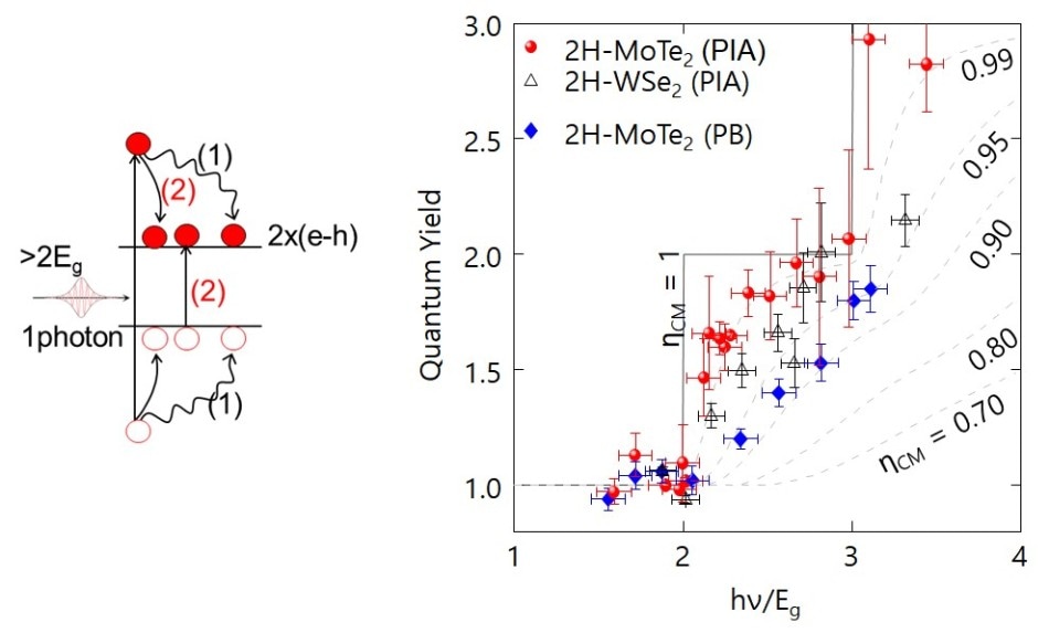
 The schematic demonstrates the photogenerated carriers with carrier multiplication (CM). The discovery of the highest CM efficiency and the lowest CM threshold energy are displayed in the quantum yield data for 2H-MoTe2 and 2H-WSe2 thin films. Image Credit: Institute for Basic Science.
The new findings have been reported in Nature Communications and have the potential to promote the photovoltaics and photodetector fields. The results could also enhance the efficiency of solar cells developed using these ultrathin materials to nearly 46%.
The van der Waals layered transition metal dichalcogenides (2D-TMDs) are an exciting group of 2D materials predicted to create the next generation of optoelectronic devices, such as transistors, solar cells, light-emitting diodes (LED), etc. They are formed of individual thin layers isolated by very weak chemical bonds (van der Waals bonds) and possess high light absorption property, unique optical properties, and high carrier (electron and hole) mobility.
Apart from enabling their bandgap to be tweaked by altering composition and layer thickness, these materials also provide an ultrahigh internal radiative efficiency of more than 99%, supported by the removal of surface flaws and large binding energy between carriers.
In general, the absorption of sunlight in semiconducting 2D-TMD monolayers reaches 5%–10%, which is an order of magnitude greater than that offered by most standard photovoltaic materials, like cadmium telluride, silicon, and gallium arsenide.
However, regardless of these optimal characteristics, the highest power conversion efficiency of 2D-TMDs solar cells has been less than 5% because of losses at the metal electrodes. The IBS researchers collaborated with scientists at the University of Amsterdam to resolve this problem by investigating the CM process in these materials.
CM is a highly efficient way to change light into electricity. A single-photon typically stimulates a single electron, leaving behind an “empty space” (hole). But it is possible to produce two or more electron-hole pairs in specific semiconductors if the energy of the incident light is adequately large, more precisely, if the photon energy is twice the bandgap energy of the material.
While the CM phenomenon is quite ineffective in bulk semiconductors, it was predicted to be very efficient in 2D materials, but was not demonstrated experimentally because of a few technical restrictions, such as ultrafast optical measurement and proper 2D-TMD synthesis.
In this research, the team evidenced CM in 2D-TMDs, such as 2H-WSe2 and 2H-MoTe2 films, for the first time. It is expected that this discovery will enhance the present efficiency of 2D-TMD solar cells, even exceeding the Shockley-Queisser limit of 33.7%.
Our new results contribute to the fundamental understanding of the CM phenomenon in 2D-TMD. If one overcomes the contact losses and succeeds in developing photovoltaics with CM, their maximum power conversion efficiency could be increased up to 46%. This new nanomaterial engineering offers the possibility for a new generation of efficient, durable, and flexible solar cells.
Young Hee Lee, Director, CINAP