Jan 27 2020
Scientists have produced an ultra-thin and ultra-flexible electronic material for the future touchscreens. This material is capable of being printed and rolled out like newspaper.
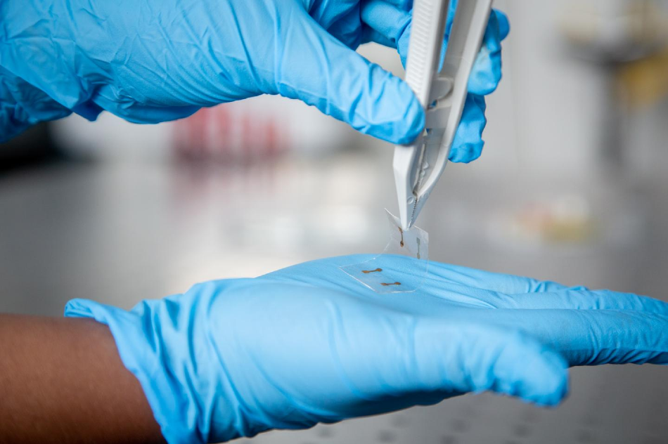
 A sample of the ultra-thin and ultra-flexible electronic material that could be printed and rolled out like newspaper, for the touchscreens of the future. Image Credit: RMIT University.
The new touch-responsive technology is 100 times thinner compared to current touchscreen materials and is highly flexible, enabling it to be wound like a tube.
Researchers from RMIT University prepared the new conductive sheet using a thin film commonly present in cell phone touchscreens and reduced it from three dimensions (3D) to two dimensions (2D) by liquid metal chemistry.
These nano-thin sheets can be readily incorporated into present electronic technologies. Thanks to their unbelievable flexibility, they can potentially be produced by roll-to-roll (R2R) processing much like a newspaper.
The study, performed together with researchers from UNSW, Monash University, and the ARC Centre of Excellence in Future Low-Energy Electronics Technologies (FLEET), was reported in Nature Electronics.
According to Dr Torben Daeneke, lead researcher, a majority of the cell phone touchscreens were formed from a transparent material, such as indium-tin oxide (ITO), which was not only very conductive but also highly brittle.
“We’ve taken an old material and transformed it from the inside to create a new version that’s supremely thin and flexible,” stated Daeneke, an Australian Research Council DECRA Fellow at RMIT.
You can bend it, you can twist it, and you could make it far more cheaply and efficiently that the slow and expensive way that we currently manufacture touchscreens. Turning it two-dimensional also makes it more transparent, so it lets through more light. This means a cell phone with a touchscreen made of our material would use less power, extending the battery life by roughly 10%.
Dr Torben Daeneke, Australian Research Council DECRA Fellow, RMIT University
DIY: A Touchscreen You Can Make at Home
The existing method for producing the transparent thin-film material used in standard touchscreens involves a slow, energy-intensive, and costly batch process, performed in a vacuum chamber.
The beauty is that our approach doesn’t require expensive or specialised equipment—it could even be done in a home kitchen. We’ve shown its possible to create printable, cheaper electronics using ingredients you could buy from a hardware store, printing onto plastics to make touchscreens of the future.
Dr Torben Daeneke, Australian Research Council DECRA Fellow, RMIT University
Thick and Thin: How to Turn an Old Material New
The scientists used a liquid metal printing technique to develop the new kind of atomically thin ITO. When heated to 200 °C, the indium-tin alloy becomes liquid, which is later rolled over a surface to print off nano-thin sheets of ITO.
Such 2D nano-thin sheets have the same chemical composition as typical ITO but a different crystal structure, providing them interesting new optical and mechanical properties.
In addition to being completely flexible, this new kind of ITO absorbs just 0.7% of light than the standard conductive glass that absorbs 5%–10% of light. By adding more layers, it can be made more electronically conductive.
It’s a pioneering approach that cracks a challenge that was considered unsolvable. There’s no other way of making this fully flexible, conductive and transparent material aside from our new liquid metal method. It was impossible up to now—people just assumed that it couldn’t be done.
Dr Torben Daeneke, Australian Research Council DECRA Fellow, RMIT University
Patent Pending: Bringing the Tech to Market
At present, the researchers have used the new material to make an active touchscreen, as a proof-of-concept, and have filed for a patent for the technology.
This new material could also be used in various other optoelectronic applications, like touch displays and LEDs, and potentially in future smart windows and solar cells.
Daeneke added, “We’re excited to be at the stage now where we can explore commercial collaboration opportunities and work with the relevant industries to bring this technology to market.”
The study was supported by the RMIT Microscopy and Microanalysis Facility (RMMF), RMIT’s MicroNano Research Facility (MNRF), the National Computational Infrastructure National Facility, the Pawsey Supercomputer Centre, and the Melbourne Centre for Nanofabrication (MCN) in the Victorian Node of the Australian National Fabrication Facility (ANFF).