Apr 28 2020
As demand for higher-efficiency and smaller electronics grows, so does demand for a new generation of materials that can be printed at ever smaller dimensions. Such materials are critical to national security applications and space exploration. But materials that work well on Earth don’t always hold up well at high altitudes and in space. Scientists are now creating new metal-based nanomaterials for circuit boards that could be resistant to the high-altitude radiation encountered by electronics in aerospace equipment, fighter jets and weapon systems.
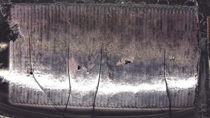
 After being bombarded with ionizing radiation, this sample with copper-platinum nano-ink on its surface still conducts electricity. Image Credit: Sandia National Laboratories
The researchers are presenting their results through the American Chemical Society (ACS) SciMeetings online platform.
“This research grew out of the huge need at U.S. national laboratories for electronic materials that are stable when subjected to ionizing radiation,” says Timothy J. Boyle, Ph.D., the project’s principal investigator. “We started looking at nanometal materials because they can be printed at the required smaller dimension, but we had to overcome their tendency to be damaged by ionizing radiation.”
Ionizing radiation comes from a variety of natural and manmade sources, and it can change the structures of molecules. On Earth, most of this radiation comes naturally from the environment, or even from the sun or outside of the solar system, and is not normally harmful. But at very high altitudes — such as those experienced by airplanes or spacecraft — the levels of radiation are much higher and can affect humans, as well as materials, that are exposed to it for long periods.
Boyle says that copper was an obvious choice to miniaturize electronics for high-altitude applications, because it has already been used in nano-inks in circuits, and it is a lower-cost alternative to more expensive materials, such as silver and gold. But like most metals, copper is susceptible to damage from elevated levels of radiation. To create new nano-inks that might hold up well in high altitudes, Boyle, Fernando Guerrero and others added, or doped, more than 10 different metals in copper to see which one would work best. They placed the metals inside the face-centered-cubic (fcc) crystal structure of copper — a cube with an atom of copper at each corner and an empty space in the center.
The group, located at Sandia National Laboratories, had to surmount numerous hurdles in synthesis, characterization, formulation and testing of the nano-inks. “We had to find a system that worked for each potential metal,” Guerrero says. “It also was challenging to insert the metal into the copper fcc and synthesize the doped metal alloy in sufficient quantity to make enough ink to print.” When Guerrero used platinum as the dopant, he finally obtained enough nano-ink to work with.
To test the copper-platinum nano-ink, Guerrero printed and sintered it in a furnace at about 700 F for an hour. Sintering compacts particles and creates a solid mass of material by heat (as in this case) or pressure. He then exposed this material to high-energy radiation in a unique instrument developed at Sandia by Khalid M. Hattar, Ph.D., called the in-situ irradiation transmission electron microscope (I3TEM). This instrument bombards the sample with ionizing radiation — similar to the type encountered by electronics operating in space or at high altitudes — while displaying it under a microscope.
“The preliminary results are promising,” Guerrero says. “The sample after exposure to the I3TEM still conducted electricity, suggesting it was resistant to the radiation.”
The next step is to test the materials to confirm the results using Sandia’s gamma irradiation facility (GIF), which provides a high-fidelity simulation of nuclear radiation environments for materials and component testing. GIF can produce a wide range of gamma radiation environments and can irradiate objects as small as electronic components and as large as an M1 Abrams tank.
“Our ultimate goal is to develop enhanced radiation-stable, copper-based electronic nanomaterials to meet munition, aerospace and nuclear monitoring needs,” Boyle says. “Our future research will focus on mastering and making smaller, more effective nanoparticles and inks and testing the printed circuits with the GIF.”
The researchers acknowledge funding from Sandia National Laboratories.