Jun 4 2021
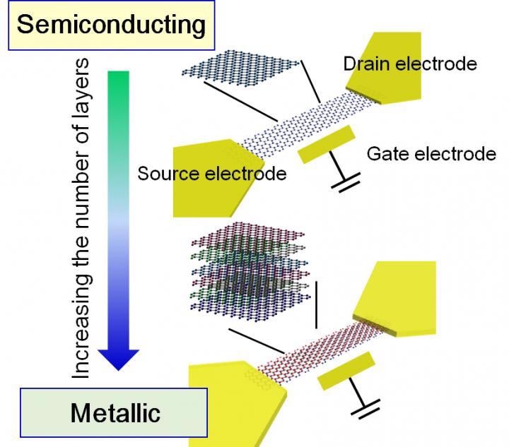
Scientists from Osaka University, in association with the Toyo University and the Kyushu Institute of Technology, have elucidated the expression mechanism of metallic and semiconducting properties in graphene nanoribbons (GNRs) by studying the carrier transport characteristics in the field-effect transistor (FET) through a multilayer GNR channel.
 Carrier transport characteristics of the FETs using the GNR channel. Image Credit: Osaka University.
Using a solid template, the researchers created multilayer GNRs with accurately regulated numbers of layers through a chemical vapor deposition method.
This enabled us to compare the observed carrier transport properties in the FET using a multilayer GNR channel with various numbers of layers and device simulations based on theoretical calculations.
Ryota Negishi, Study First Author, Osaka University
The study revealed that the carrier transport behavior of the FET-GNR varies from semiconducting to metallic characteristics, such as semiconducting behavior for some layers (1 to 3 layers) and metallic behavior for multilayers (6 to 8 layers) as shown in the above image.
This is because the impact of the charged impurities on the device substrate (SiO2/Si) is decreased.
The above image depicts the surface potential map of the multilayer and monolayer graphene estimated by the simulation of the device.
In this example of monolayer GNR, the local high potential barriers are created by the charged impurities on the substrate; but in the example of multilayer GNRs, the surface potential becomes flat because of the field screening effect present between the layers.
The above image schematically displays the surface potential of multilayer and monolayer GNRs. The local high potential barriers affect the carrier transport of the monolayer GNR on the device substrate because of the charged impurities and thus exhibits hopping conduction over the barriers supported by thermal energy.
Particularly, the conduction electrons in a thin 1D structure, like a monolayer GNR, are localized and display properties similar to semiconductors because the locally created potential barriers split the current pass of the thin GNR channel.
By contrast, in the case of a multilayer GNR, the electric field of the charged impurities is considerably decreased as the number of layers increases because of the screening effect between the layers, and the potential close to the top layer becomes flat and displays the metallic properties with high conductivity.
The above image also depicts the observed carrier transport characteristics of the FET with the GNR channel as a function of the number of layers. Once the number of layers reaches about five, the carrier transport properties change from semiconducting to metallic characteristics.
A five-layer film thickness agrees well with the screening length (approximately 1.5 nm) of the electric field because of the charged impurities present on the substrate. This shows that carrier transport properties (that is, metallic and semiconducting characteristics) in real GNR devices are governed by the presence or absence of environmental impacts.
We have succeeded in controlling semiconducting and metallic properties of FETs using multilayer GNRs by modulating the number of layers. GNRs with excellent carrier transport properties are attracting attention as next-generation electronic device materials.
Ryota Negishi, Study First Author, Osaka University
“This study provides design guidelines for GNRs that incorporate actual device structures. This achievement is an important milestone that will accelerate the application of GNR materials for purposes such as high-speed transistors and ultra-thin wiring,” Negishi concluded.
Journal Reference:
Negishi, R., et al. (2021) Crossover point of the field effect transistor and interconnect applications in turbostratic multilayer graphene nanoribbon channel. Scientific Reports. doi.org/10.1038/s41598-021-89709-z.