In an article recently published in the journal Nanotechnology, researchers employed a single particle imaging method for fluorescence excitation with moderate intensity to achieve spatial resolution. Here, the semiconductor nanocrystals were accessed, whose emission lifetimes depended on excitation intensity.

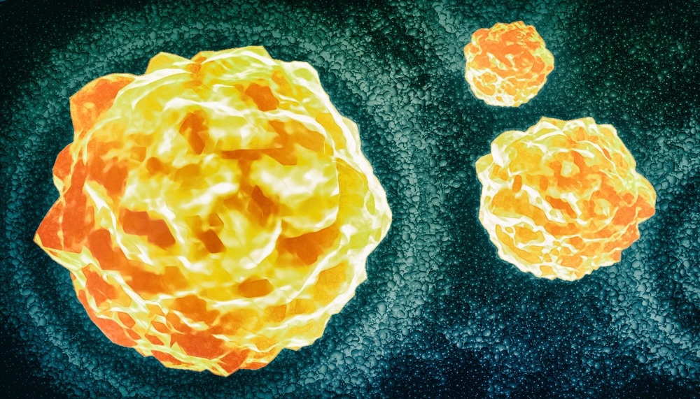
Study: Excited state lifetime modulation in semiconductor nanocrystals for super-resolution imaging. Image Credit: GiroScience/Shutterstock.com
Nanocrystals
The excited fluorophore's de-excitation rate with optical modulation is an important tool to achieve super-resolution in microscopy techniques, including ground state depletion microscopy, stimulated emission depletion, or reversible saturable optical fluorescence transitions microscopy.
In organic dyes or fluorescent proteins, the excitation methods involve transition rate tailoring from a single excited to a ground state. However, semiconductor nanocrystals intrinsically possess multiple excited states, grey or charged states.
The excessive energy stored either in the nanocrystal core or trapped in the bulk of the nanocrystal or at its surface results in the origin of multiple states. Wavefunction overlap of an exciton with trapped charges can increase the non-radiative energy transfer probability from the exciton to the charge. Thus, the exciton's excited-state lifetime decreases based on the location and amount of charge trapped within the particle.
Semiconductor Nanocrystals for Super-Resolution Imaging
In the present study, the researchers used the semiconductor nanocrystal's excitation-intensity-dependent lifetime to increase the spatial imaging resolution beyond the diffraction limit. A single semiconductor nanocrystal was scanned through a confocal spot with a diffraction limit to modulate the excitation power density, which is maximum at the center and minimized towards the edges. Thus, several photo-generated excess charges in a particle can be modulated; consequently, its excited-state lifetime is also modulated.
The lifetime modulation relative to the position of a particle according to the focused laser allowed the enhancement of the spatial resolution in the scanned image of the nanocrystal. This was demonstrated by two close-by emitter images' disentanglement, which remained unresolved in the intensity image. This method combined the simplicity and robustness of the measurement technique that combines the laser-scanning confocal microscope with fluorescence-lifetime measurement capability.
Research Findings
The researchers used cadmium selenium (CdSe) /cadmium sulfur (CdS) / thick-shell quantum dots (QDs); the shell thickness helped reduce fluorescence blinking. A transmission electron microscopy (TEM) image showed that the average particle size is in the range of 18 ± 2 nanometers, which included a CdS shell consisting of approximately 15 atomic layers. In this type of giant QDs, the interaction between excited-state carriers and surface trap states was weakened, further suppressing the non-radiative Auger recombination. Fluorescence blinking was suppressed by reducing the Auger efficiency and hot-carrier capture. If not suppressed, blinking could lead to patchy single-particle confocal scan images, which reduce the particle's localization accuracy.
The radially polarized laser beam was used to scan semiconductor nanocrystals with the diffraction-limited focal spot. Herein, the radial polarization majorly led to axially polarized excitation of the approximate diameter of 180 nanometers at a wavelength of 640 nanometers. This enhanced the diffraction-limited resolution by approximately 1.4 times compared to a linearly polarized Gaussian beam.
Multichannel picosecond event timer-equipped confocal microscope was used for all fluorescence measurements, allowing fluorescence lifetime imaging. To focus the excitation light and collect the fluorescence light, a high numerical aperture objective was equipped for the system. As an excitation source, a white-light laser system with an acousto-optical tunable filter was used. A non-polarizing beam splitter reflected the excitation light towards the objective. Calculations for average excited state lifetime were performed by fitting the fluorescence decay curves with a multi-exponential decay model.
The characteristic intensity pattern, shown from the single quantum emitter's recorded scan image depended on the orientation of the dipole moment of fluorophore's excitation. However, the three-dimensional (3D) excitation isotropy of spherical semiconductor nanocrystals avoided the dependency of the excitation pattern on the orientation.
The semiconductor nanocrystal's fluorescence lifetime that depended on the excitation power allowed the narrowing of the particle's fluorescence lifetime image compared to the diffraction-limited intensity image.
The non-additivity of lifetimes depended on sigmoid curve steepness at its inflection point and the number of detected photons determining the fluorescence decay curve fitting quality. Further, the non-additivity of lifetimes resulted in the resolution enhancement. However, both curve steepness and photons quantity depended on the experimental conditions, including QD's optical properties and microscope parameters.
Conclusion
In conclusion, the researchers presented the proof-of-principle measurements for semiconductor nanocrystal excitation-intensity-dependent, lifetime modulation-based, super-resolution imaging method. They showed that this method allowed to achieve a ten times resolution at moderate fluorescence intensities, which further could be enhanced by more photons collection.
This method employed a conventional fluorescence-lifetime confocal microscope based on semiconductor nanocrystal's fluorescence lifetime imaging to access a broad fluorescence microscopy community. Although the present work involved the excitation by using a radially polarized laser beam, a linearly polarized Gaussian beam can also be used for excitation with minimized focus diameter.
Reference
Ghosh, S., Hollingsworth, J., Gallea, J. I., Majumder, S., Enderlein, J., and Chizhik, A. (2022). Excited state lifetime modulation in semiconductor nanocrystals for super-resolution imaging. Nanotechnology. https://iopscience.iop.org/article/10.1088/1361-6528/ac73a2
Disclaimer: The views expressed here are those of the author expressed in their private capacity and do not necessarily represent the views of AZoM.com Limited T/A AZoNetwork the owner and operator of this website. This disclaimer forms part of the Terms and conditions of use of this website.