More potent, portable gadgets have been developed as a result of the ongoing miniaturization of electrical technologies. These technological innovations, like artificial intelligence, social networks, telemedicine, and 5G networks, are made possible in large part by these electronic devices, including smartphones and laptops. They have made the 21st century a sharper and more networked era.
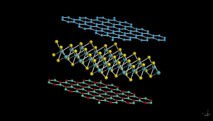
 Van der Waals heterostructures, as seen in the image, can be formed via ‘LEGO-stacking’ of different 2D materials. Image Credit: Singapore University of Technology and Design
The advancement of electronics into the nanoscale domain, where a nanometer is 10,000 times thinner than a human hair strand, also poses enormous technological difficulties. Due to the emergence of a strange quantum mechanical phenomena that rules the nanoscopic universe, silicon, a crucial component of modern electronics, begins to behave erratically.
As a result of this, it is necessary to significantly thin down silicon nanoelectronics to manage the quantum effect and better control the device. However, silicon nanoelectronics production requires sophisticated technology. If the “thinning down” procedure is not done correctly, silicon’s electrical characteristics can frequently suffer serious degradation.
Two-dimensional (2D) materials, a class of ultra-thin materials with a thickness of only a few atoms, offer fresh possibilities for the never-ending search to further miniaturize electronic devices.
Devices made of 2D material provide remarkable controllability even at the nanometer scale thanks to their intrinsically ultra-thin body. Scientists and engineers have demonstrated their potential in an array of advanced device technology applications, including faster, less energy-hungry, flexible, highly compact, and even brain-mimicking devices.
More interestingly, various 2D material species can be “LEGO-stacked” into a van der Waals heterostructure (vdWH). The component materials’ physical properties are merged, resulting in new “designer” physical properties that are not conveniently found in natural crystals.
The vdWH method significantly increases the operational device design flexibility of 2D materials. The multiferroic version, in which 2D materials with fundamentally exceptional properties are merged, is an especially compelling and technologically significant class of vdWH.
A magnetic 2D material, for instance, can be merged with another ferroelectric 2D material, the electrical behavior of which can be tuned from outside via a voltage signal. The subsequent multiferroic VdWH can then exhibit voltage switchable magnetism, a property that is extremely useful in computing electronics and memory devices.
The accomplishment of multiferroic vdWH construction is critically dependent on the selection of suitable materials. Despite the high demand for 2D-material-based multiferroic vdWH, the extensive investigation for functional multiferroic vdWH has yielded only a few prototypes with adequately great prospects for electronics device application.
Using state-of-the-art computational simulation, the team of researchers led by the Singapore University of Technology and Design (SUTD) created a multiferroic vdWH with strong capability in memory and spin-based computer systems.
The team discovered that by layering a magnetic 2D material, FeCl2, and a ferroelectric 2D material, Sc2CO2, the magnetism of the resulting multiferroic vdWH could be quickly transitioned using a voltage signal.
The most optimal stacking setups and material combinations are acquired through a thorough and rigorous computational exploration. These results can be used to develop design guidelines for future experimental fabrication, device prototyping, and advancements in spintronic technology.
Spintronics is a new device concept that works on a completely different principle than traditional electronics technology. Spintronic devices are expected to facilitate ultrafast computation while ingesting much less energy by utilizing the “spin” of an electron—a complex quantum mechanical property.
The research group proved that the multiferroic vdWH in this work could be used as spin polarizers, a critical building block of spintronic technology, using a nanodevice simulation.
Although multiferroic systems have been widely studied using bulky materials, the 2D material counterpart studied in this work has the potential of ultimately compact multiferroic devices, which could be very useful for ultracompact memory devices. The ability to host a spin-polarized current further suggests that the system can also be a candidate material for spintronic technology.
Dr. Yee Sin Ang, Study Lead and Assistant Professor, Singapore University of Technology and Design
“The multiferroic vdWH designed in this project offers an interesting route for the development of high-performance computing electronics with minimal energy consumption, thus paving an important first step towards a more sustainable future computing electronics technology,” added Ang.
Journal Reference:
Cao, L., et al. (2022) Multiferroic van der Waals heterostructure FeCl2/Sc2CO2: Nonvolatile electrically switchable electronic and spintronic properties. Physical Review B. doi.org/10.1103/PhysRevB.105.165302.