Sep 12 2007
Oxford Instruments, the high-technology tools and systems company, and NIL Technology®, the nanotechnology company located in Kongens Lyngby, Denmark, have collaborated to develop etch processes targeted specifically at nanoimprint lithography.
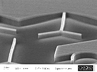
 SEM image of optimised fused silica stamp etch (30 nm features to 200 nm depth)
Nanoimprint lithography is a versatile, cost effective, flexible and high throughput method for fabrication of down to and below 10 nm structures with a wide range of application within, for example, data storage, optics and bio-sensors.
The collaboration combined Oxford Instruments’ process development expertise in plasma etching with NIL Technology’s experience in developing and supplying templates, stamps and processes for nanoimprint lithography. Together the companies have developed processes for the etching of nanoimprinting stamps in fused silica, de-scumming of the imprinted polymer with negligible critical dimension (CD) loss, and etch of the final structure.
The etch developments were carried out using Oxford Instruments’ PlasmaLab System100 inductively coupled plasma (ICP) tool. ICP etch shows superior capabilities for etching of high performance NIL stamps with well-controlled profiles. The stable low pressure de-scum process possible with ICP effectively removes residual polymer after imprinting with minimal loss of CD, and ICP is also perfect for transferring the imprinted pattern into fused silica and silicon.
Brian Bilenberg, Chief Technical Officer of NIL Technology, comments, “We saw an opportunity for NIL Technology and Oxford Instruments to work together to develop processes which are optimised as an overall end-to-end process rather than in individual steps. As we continue further work, we expect to improve the whole process of etching nanostructures created by nanoimprint lithography yet more.”