May 28 2008
Carbon nanotubes, described as the reigning celebrity of the advanced materials world, are all the rage. Recently researchers at Rice University and Rensselaer Polytechnic Institute used them to make the “blackest black” — the darkest known material, reflecting only 0.045 percent of all light shined on it.
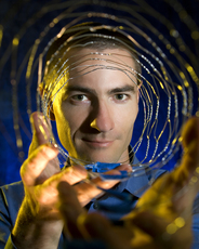
 When Sandia's Francois Leonard explains the physics of carbon Leonard has written a book on the subject to be published later this summer
Sandia National Laboratories is also in on the carbon nanotube game, with research led by physicist François Léonard. Léonard has considerable experience in the subject, so much that he wrote the book on it — literally. He’s the author of a forthcoming work, Physics of Carbon Nanotube Devices, which could become the definitive text on the topic.
Carbon nanotubes are long thin cylinders composed entirely of carbon atoms. While their diameters are in the nanometer range (1-10), they can be very long, up to centimeters in length. The carbon-carbon bond is very strong, making carbon nanotubes very robust and resistant to any kind of deformation. The properties of other single-element materials are obvious — gold is a metal and silicon is a semiconductor, for example. Carbon nanotubes, on the other hand, have a sort of dual personality not found in other materials made from a single element. They’re special because they can be either metallic or semiconducting.
Léonard explains that this results from the actual structure of a carbon nanotube; the way the atoms are arranged around the tube determines its electronic properties. To explain this concept to a group of undergraduates at the University of California, Berkeley, he uses three rolls of chicken wire, each cut at a different angle. The chicken wire represents the sheet of graphene from which the nanotube is cut. The angle of that cut creates a different bond geometry along the nanotube, which results in different properties.
Working in uncharted territory
Léonard’s experience with carbon nanotubes began when the field was just emerging. While the discovery of carbon nanotubes is credited to Japanese physicist Sumio Iijima in 1991, work on applications didn’t begin until the late 1990s. Léonard was at IBM as a postdoc when researchers there built the first transistor from carbon nanotubes.
As a theoretical physicist, Léonard was working in uncharted territory. From the beginning, he worked on modeling approaches to understand how carbon nanotubes might behave in certain applications. He joined Sandia in 2000, where he has continued his carbon nanotube research.
The semiconducting side of carbon nanotubes holds a lot of promise for the development of new nanoelectronic devices. “A carbon nanotube creates a transistor that is only one nanometer wide,” says Léonard. “This makes it possible, in principle, to achieve very high device densities compared with the current state of the art.” The field emission properties of carbon nanotubes are also exciting. Flat panel displays are typically made from a high density of sharp tips, to which high voltage is applied to extract electrons. These electrons strike and activate the pixels in the screen. Carbon nanotubes can serve this purpose because they are very sharp, long, and can sustain high fields and high temperatures.
‘Layla’ on a nanotube receiver
Researchers have demonstrated the ability to assemble such devices with a single carbon nanotube. At a recent conference, one scientist played Eric Clapton’s “Layla” on a carbon nanotube device acting as a radio receiver.
Another potential use is in chemical and biological sensors. Carbon nanotubes, because of their small diameter, can serve as very sensitive detectors, with the ability to detect a single molecule of a target substance. DNA detection has also been demonstrated. Currently, Léonard is leading a team to develop optical detection using carbon nanotubes. The project is a partnership with Lockheed Martin.
Unique electronic properties
Semiconducting carbon nanotubes have many properties that make them attractive for optical detection. They have unique electronic properties that favor light absorption. In addition, the wavelength over which light is absorbed can be controlled with nanotubes of different diameters. Importantly, the device fabrication process could be entirely compatible with fabrication processes used by the semiconductor industry. In addition to carbon nanotubes, Léonard is interested in electronic transport in other nanostructures — carbon nanotubes as well as nanowires and single molecules. The question, he says, is how does current pass across nanostructures? How is transport of electrons different than in conventional materials?