Dec 2 2008
Applied Materials, Inc. today unveiled its Applied Centura® Enabler® E5 dielectric etch system, the industry’s most advanced solution for creating the 40:1 high aspect ratio contact features that are critical to the yield and performance of 32nm and below DRAM and Flash memory chips. The Enabler E5 sets a new benchmark in profile control, enabling customers to manufacture high performance, robust, next-generation memory devices with >80% bottom-to-top CD ratios across the wafer, and with less than 3nm bowing of the contact sidewall.
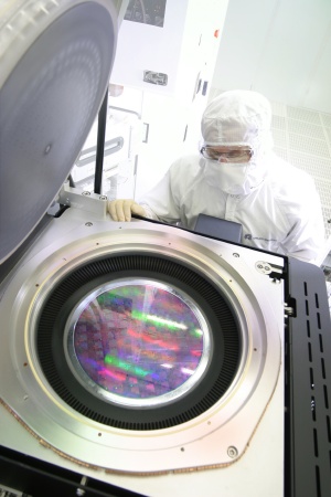
 The Applied Centura Enabler E5 sets an industry benchmark, enabling customers to etch 40:1 high aspect ratio contacts with the excellent profile control required for 32nm and below memory chip manufacturing. (Photo: Business Wire)
“Next-generation Flash and DRAM devices pose a significant challenge for dielectric etch systems since it is very difficult to achieve the global profile control necessary for fabricating high aspect ratio contacts,” said Ellie Yieh, vice president and general manager of Applied Materials’ Etch and Cleans Business Unit. “The Enabler E5 is the only system that can meet all these requirements, allowing memory manufacturers to continue to increase density and reduce the cost-per-bit.”
“Customers are very excited about the Enabler E5 system’s exceptional profile control,” added Ms. Yieh. “We’re seeing strong demand for this product with multiple systems installed worldwide and repeat orders from leading memory manufacturers where it has solidly won multiple head-to-head run-offs with other systems.”
Central to the Enabler E5 system’s performance are its unique reactor architecture and precise process control that provide repeatable, uniform vertical profiles at high aspect ratios globally – from edge-to-edge and wafer-to-wafer – addressing a critical yield inhibitor at higher memory densities. The proprietary chamber technology also provides more efficient cleaning, delivering 50% longer between-maintenance intervals than any competitive system.