Sep 6 2010
Progress on controlling the growth and doping of semiconductor nanowires makes these structures promising building blocks for nanoelectronics and nanophotonics.
They are often grown by chemical-vapor deposition using the vapor-liquid-solid mechanism, in which a metallic particle is used to catalyze the growth of the semiconductor. These nanowires are very photonic, i.e., they interact strongly with light because of their high refractive index and dimensions.
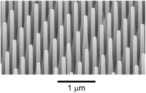
 Periodic array of indium phosphide nanowires. This sample was fabricated by defining a pattern of gold particles with substrate-conformal imprint lithography. The particles catalyze the growth of nanowires.
Development of passive photonic devices based on semiconductor nanowires and nanorods, such as waveguides and antireflective surfaces, has recently been reported. Nanowires can be grown with large aspect ratios, thus making it relatively easy to contact them in electronic devices. Active components, such as LEDs, lasers, and photodetectors based on nanowires have been demonstrated.
One of the most exciting possibilities and opportunities for nanowires is in the field of photovoltaics. Efficient extraction of photo-generated carriers is possible in radial p-n junctions or core-shell nanowires, in which the core and surrounding shell have different doping. Nanowire diameters, on the order of tens to hundreds of nanometers, are smaller than the diffusion length of the minority carriers, thus facilitating their extraction before recombination.
Much research has focused on individual nanowires. Giant anisotropy in the absorption of light has been observed, which depends on the polarization state relative to the nanowire axis. Scattering (Mie) resonances in thick nanowires have also been proposed as a means to enhance optical absorption. However, solar cells are based on large surfaces covered by dense arrays of nanowires in which multiple scattering of light is unavoidable. Therefore, understanding the scattering of light by ensembles of nanowires is critical to improve the design and optimize the performance of solar cells.
We are investigating the propagation of light through layers of semiconductor nanowires and nanorods. Our research has two goals related to photovoltaics, including improving the coupling efficiency of incident light into planar solar cells, and enhancing the efficiency and bandwidth of optical absorption by ensembles of semiconductor nanowires.
Inhomogeneous layers of short, nonabsorbing nanowires act as broadband and omnidirectional antireflection surfaces. They form an effective medium with a graded refractive index, varying from low values close to unity (i.e., the refractive index of air) to high values close to the refractive index of the underlying substrate. This graded index improves the coupling of light from air into the substrate by reducing the specular reflection. It is a consequence of the increasing filling fraction of the nanowires with depth into the layer, which stems from tapering of the nanowires during growth—see Figure 1(a)—or the distribution of nanowire lengths: see Figure 1(b). We have demonstrated that the layers' reduced reflection leads to increased transmission into the substrate and not to enhanced diffuse reflection or absorption. Incident light on the top surface is gradually coupled into the high-refractive-index substrate with minimized specular reflection.
Two advantages of nanowire antireflection surfaces (as compared to standard interference coatings) are that the former exhibit omnidirectional behavior and demonstrate a broadband response that spans the entire solar spectrum. Figure 2 illustrates the omnidirectionality of the antireflection behavior. We show transmission into a gallium phosphide (GaP) substrate covered by a layer of GaP nanowires, normalized by the transmission of a bare GaP substrate, for angles of incidence between 0 and 60°. Transmission into the substrate improves by reducing the specular reflection for all wavelengths and angles: see Figure 1(c). Although the layers in Figure 1 correspond to GaP nanowires on a GaP substrate, the hetero-epitaxial growth of nanowires on different substrates will allow fabrication of antireflecting nanowire layers on top of triple-junction solar cells.
Multiple scattering of light is not relevant in thin (submicron) layers of small nanowires. However, as the diameter and length of the nanowires is increased, scattering becomes a major effect in the transport of light. Diffuse reflection can decrease transmission into the substrate by orders of magnitude. Nevertheless, we can use scattering to our advantage by increasing the optical absorption in layers of active nanowires.
We recently demonstrated that diffuse reflection can be suppressed in random ensembles of semiconductor nanowires by optimizing the ratio between the absorption and scattering mean free paths of light. As a next step, we are controlling this scattering in defect-free periodic arrays of nanowires. These arrays are obtained by structuring a periodic catalytic surface of gold nanoparticles for the growth of nanowires, using substrate-conformal imprint lithography. This will facilitate fabrication of the large periodic arrays of nanowires necessary for photovoltaic applications.
Source: http://spie.org/