Jul 9 2013
EV Group (EVG), a leading supplier of wafer bonding and lithography equipment for the MEMS, nanotechnology and semiconductor markets, today introduced the latest version of its EVG®40NT automated measurement system, which is designed to work in concert with the company's GEMINI® FB fusion wafer bonding system to support the manufacture of next-generation 3D-integrated CMOS image sensors.
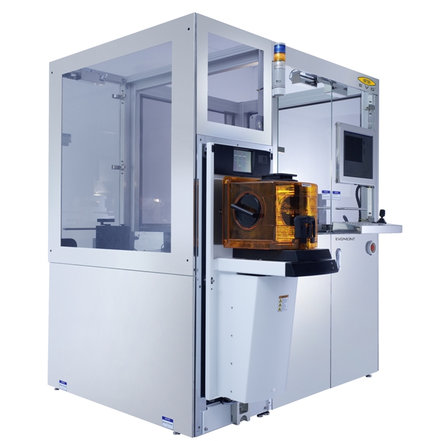
 EVG ®40NT Automated Measurement System for 3D IC manufacturing
The enhanced EVG40NT measures wafer-to-wafer alignment accuracy to within 40 nm (3 sigma), while its seamless software integration with the GEMINI FB provides a closed-loop fusion bonding control system that enables the manufacture of ultra-fine-pitch (less than two micron) through-silicon vias (TSVs). These tighter specifications are necessary for enabling the production of 3D-integrated image sensors, and pave the way for accelerating 3D-integration with other device types, such as stacked memory.
"EV Group's GEMINI FB fusion wafer bonding platform is the de facto industry standard for CMOS image sensor production, and already leads the industry in wafer-to-wafer alignment accuracy due to our proprietary SmartView® alignment technology," stated Dr. Thorsten Matthias, business development director at EV Group. "The integration of GEMINI FB with the enhanced EVG40NT brings statistical process control and alignment accuracy to a whole new level, and pushes 3D-IC manufacturing to new limits. High-precision manufacturing requires accurate metrology that is seamlessly integrated into the process to enable real-time monitoring and fast corrective action. In the case of wafer bonding, measuring and mapping each die gives valuable insight into local stress variations created during upstream processes, which can cause distortions and local misalignments further downstream."
Fusion wafer bonding is ideally suited for 3D-integrated image sensors and other stacked devices because it is a room-temperature bonding process, which eliminates misalignment due to thermal expansion mismatch between the wafers. Having the ability to inspect the quality of the wafer bond and measure alignment accuracy prior to the final annealing step provides an easy rework path, thereby enabling 100-percent yield for wafer stacking. The GEMINI FB platform combines EVG's LowTemp plasma activation technology, wafer cleaning, SmartView wafer-to-wafer alignment and fusion wafer bonding in a single fully automated high-volume-manufacturing system. The EVG40NT performs highly accurate, non-destructive, top-to-bottom side alignment accuracy measurements on double-sided structured wafers or bond interfaces, as well as critical dimension and box-in-box measurements of single and double-sided structured wafers.
"Next-generation image sensors are the technological frontrunners for 3D-IC manufacturing technology," according to Hermann Waltl, executive sales and customer support director at EV Group. "High-density TSV arrays, sub-micron-diameter TSVs and ultra-thin wafers have all been successfully transferred into high-volume image sensor manufacturing. Now that adoption of wafer-to-wafer 3D stacking for image sensors is well underway, we expect to see 3D-integration follow very soon for other devices such as stacked memory."
Media and analysts interested in learning more about EVG's latest developments in wafer bonding and other processing solutions are invited to visit the company's booth #819 in the South Hall of the Moscone Convention Center in San Francisco at the SEMICON West show this week, as well as attend the company's presentations during the show's technical program. Markus Wimplinger, corporate technology development and IP director of EV Group, will present "High Resolution In-line Metrology Module for High-Volume Temporary Bonding Applications" at the SEMATECH Workshop on 3D Interconnect Metrology on Wednesday, July 10 from 11:20 - 11:40 a.m. at the San Francisco Marriott Marquis. In addition, Dr. Thorsten Matthias, business development director at EV Group, will present "From Sensor Fusion to System Fusion" at the TechXPOT session "MEMS and Sensor Packaging for the Internet of Things" on Thursday, July 11 from 12:10 - 12:30 p.m. in the Moscone North Hall.