Jul 1 2016
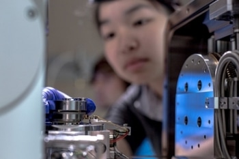
UC Merced researchers are now focused on studying the new Zeiss Gemini SEM 500 scanning electron microscope, first of its type, installed in the US. This SEM can be used for viewing extremely small things.
 (Credit: University of California, Merced)
“It’s the latest model in Zeiss’ well-established platform,” Anand Subramaniam, Professor of School of Engineering said. “This is an essential element of nanotechnology research, but it’s also important for our campus to have this kind of equipment, because it helps us teach and prepare students.”
The Imaging and Microscopy Facility (IMF), which is the main research facility operated by the Office of Research and Economic Development houses this microscope. The microscope was bought through the Merced Nanomaterials Center for Energy and Sensing (MACES) funded by NASA.
MACES, which was established in 2015, offers increasing opportunities for scientists across the university campus and for various students all through the San Joaquin Valley.
This new SEM can be used by anyone within the university campus due to the efforts of Dorothy Leland, Chancellor, and Sam Traina, Vice Chancellor for Research and Economic Development who incremented NASA’s grant funds by $150,000,.
It’s very, very high resolution. With it, we can see nanometer-scale objects. This instrument enables us to conduct enhanced nanomaterial-based research.
Jennifer Lu, Professor of the School of Engineering, and the MACES director
According to the nanoscale, a sheet of paper is around 100,000nm thick. A strand of human DNA is 2.5nm in diameter. One inch contains 25,400,000nm. A strand of human hair is around 80,000 to 100,000nm wide.
The scientists are constructing small structures for biological sensing and green-energy harvesting and transformation, and they need to have access to images of the structures they are producing. Nanoscale topography and orientation of nanoscale objects can be viewed through this new microscope.
The nanoscale features that could not be visualized even with the greatest-resolution light microscope, can be seen through the electron beam. The SEM is set up in a soundproof, vibration-minimizing lab equipped with specific metal plates that maintain the room free from external interference in order to guarantee maximum performance.
We had to put the lab where it is, because if it were closer to the outside of the building, even a large truck going by could pull the electron beam away from its target.
Mike Dunlap, lab manager
MACES chose this model as it features industry leading resolution and is extremely user-friendly, said the professors. Beginners can get functional images having nanoscale resolution from specific sample types within one hour, under the guidance of an intermediate user, said Subramaniam.
The public would be able to have a glimpse of the microscope at an open house co-hosted by Zeiss and MACES on July 14, Zeiss commented. There would be various other public events all through the year, but scientists have already started to use the SEM with good results, Professor Tao Ye stated.
Though graduate students majorly use this advanced instrument, SEM would also be beneficial to undergraduate training and professional development programs for high school teachers conducted by MACES.
A group of seven Merced College and California State University students have been guided by the center for a two-month summer internship. Lu and his colleagues, the other MACES-affiliated faculty would guide the students for learning correct lab procedures and obtaining hands-on experience in constructing nanomaterials, which include the usage of the new SEM.
MACES provides summer opportunities to raise the number of students who select science, technology, engineering and math (STEM) paths with the aim of increasing the Valley’s highly skilled workforce.
Through rigorous training, our goal is to prepare Ph.D. graduates who will evolve as major contributors to NASA’s mission. We’re also promoting and cultivating research efforts between our faculty members and graduate and undergraduate students from UC Merced and beyond.
Lu