Feb 9 2011
Altatech Semiconductor S.A. has received an order for its versatile AltaCVD platform from the Fraunhofer Research Institution for Modular Solid State Technology EMFT in Munich, Germany.
The 200-mm AltaCVD system was selected for its ability to perform both plasma-enhanced and sub-atmospheric-pressure CVD processes, which the Fraunhofer center will use in depositing dielectric layers and layer stacks on silicon and silicon-on-insulator (SOI) wafers.
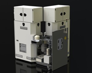
 AltaCVD 200 System
The AltaCVD platform's flexible architecture allows it to be used for sub-atmospheric-pressure deposition (SACVD) of ultrathin conformal isolation layers inside deep vias and trenches with aspect ratios as high as 40:1. When used in plasma-enhanced deposition (PECVD) mode, the system can create doped silicon-oxide films used in planarizing advanced CMOS structures. All process steps run at low temperatures between 150 degrees C and 430 degrees C to reduce thermal stresses and improve yields.
The AltaCVD 200 tool will be installed at Fraunhofer EMFT by the second quarter of 2011, with continuing applications support provided by Altatech Semiconductor's local technical team, based in Dresden.
"Our highly flexible AltaCVD platform continues to generate orders from R&D leaders and chipmakers around the world. We are pleased with the acceptance of the reactor for high-k oxide and metal deposition processes and low-temperature TSV films," said Jean-Luc Delcarri, president of Altatech Semiconductor.
Source: http://www.altatech-sc.com/